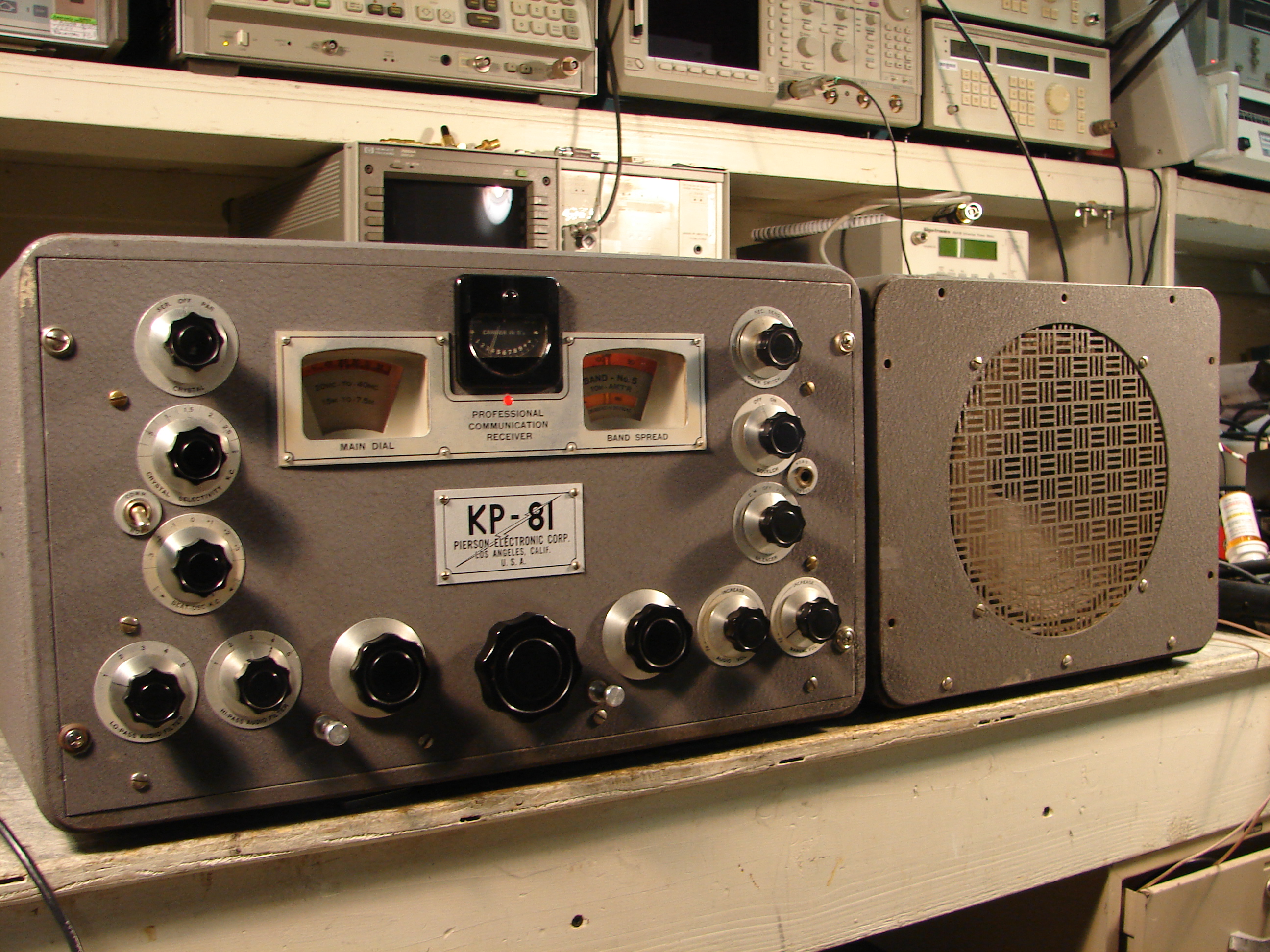
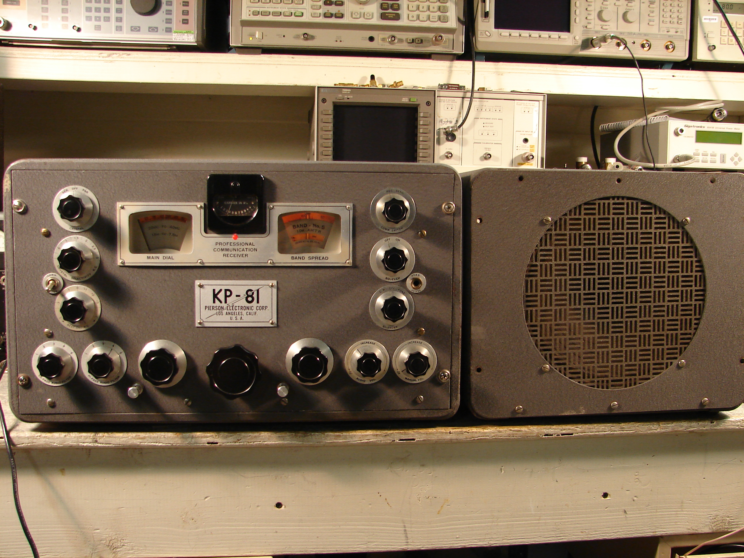
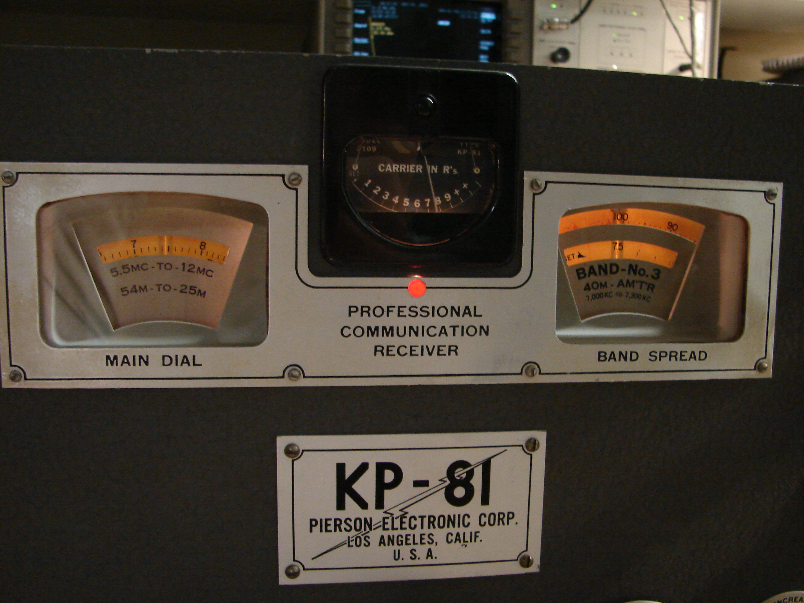
Restoring a Pierson KP-81
by John Vendely K9WT
September 2011
Toward the end of World War II, noted radio engineer Karl E. Pierson undertook the development of what he hoped would be a general coverage communications receiver of the highest quality, suitable for professional as well as amateur use. Utilizing knowledge Pierson gained during his wartime radio development work, and incorporating the best electrical and mechanical design features of the day, the result was the Pierson KP-81 receiver. First offered for sale in 1946 in the midst of an economic downturn, the KP-81 was a technical success, but was difficult and expensive to manufacture. The Pierson Electronic Corporation was apparently unable to produce the receiver profitably, even at its exorbitant selling price of nearly $400. Furthermore, there was considerable competition from low cost war surplus receivers beginning to flood the market. Regrettably, the KP-81 remained in production for only about one year, and only a few hundred sets were ever produced before Pierson Electronic Corporation failed some time in 1948.
Because of its high quality, a surprising number of KP-81 receivers still exist today. But the process of maintaining and restoring these 65 year old receivers is complicated by the lack of good service literature. The KP-81 design evidently was in flux during most of its short production life, and as a result only a preliminary technical manual was issued, containing little useful service information. Schematics showed no component values, no parts list was provided, and no service or alignment procedures were included. It is possible that no two receivers were built exactly alike. A comprehensive manual with updated schematics and parts lists was promised, but none is known to have been issued.
Given the scarce technical data on the KP-81, it seemed a shame to proceed with restoration without documenting the receiver in the process. As a result, I decided to try to develop some useful technical documentation as I worked through the complete restoration of a KP-81. I first compiled a parts list by direct inspection of the entire receiver after complete disassembly. The parts list represents the components found in receiver serial number 2012 which, based on a date stamp inside its cabinet, was produced on or about June 7, 1947. Reference designators are those of the schematic included with the original KP-81 owner’s manual, a copy of which was graciously posted to the Boat Anchor Manual Archive website by Rodger Singley, WQ9E. Persons interested in the KP-81 should begin by downloading a copy of this manual. The original schematic contains numerous errors, such as several duplicate reference designators and a few differences in circuit configuration. In addition, a few items on the schematic are illegible. I have annotated the parts list in an attempt to clarify the discrepancies. Overall, the schematic agreed surprisingly well with the actual circuitry found in receiver number 2012, though other sets may differ, particularly the later ones.
In addition, I compiled some information based on my experiences during the overhaul process, including general description and performance impressions, circuit analysis, alignment procedures, certain disassembly procedures, and notes on overhaul and a few pre-purchase inspection suggestions. These are by no means comprehensive. Rather, they are attempts to cover topics I thought would be of primary interest and importance to the restorer. Contributions of additional technical and historical information from other KP-81 owners will be gladly received.
I hope this information will fill some of the gaps in the existing KP-81 literature, and will stimulate interest in, and simplify the process of restoring these remarkable receivers.
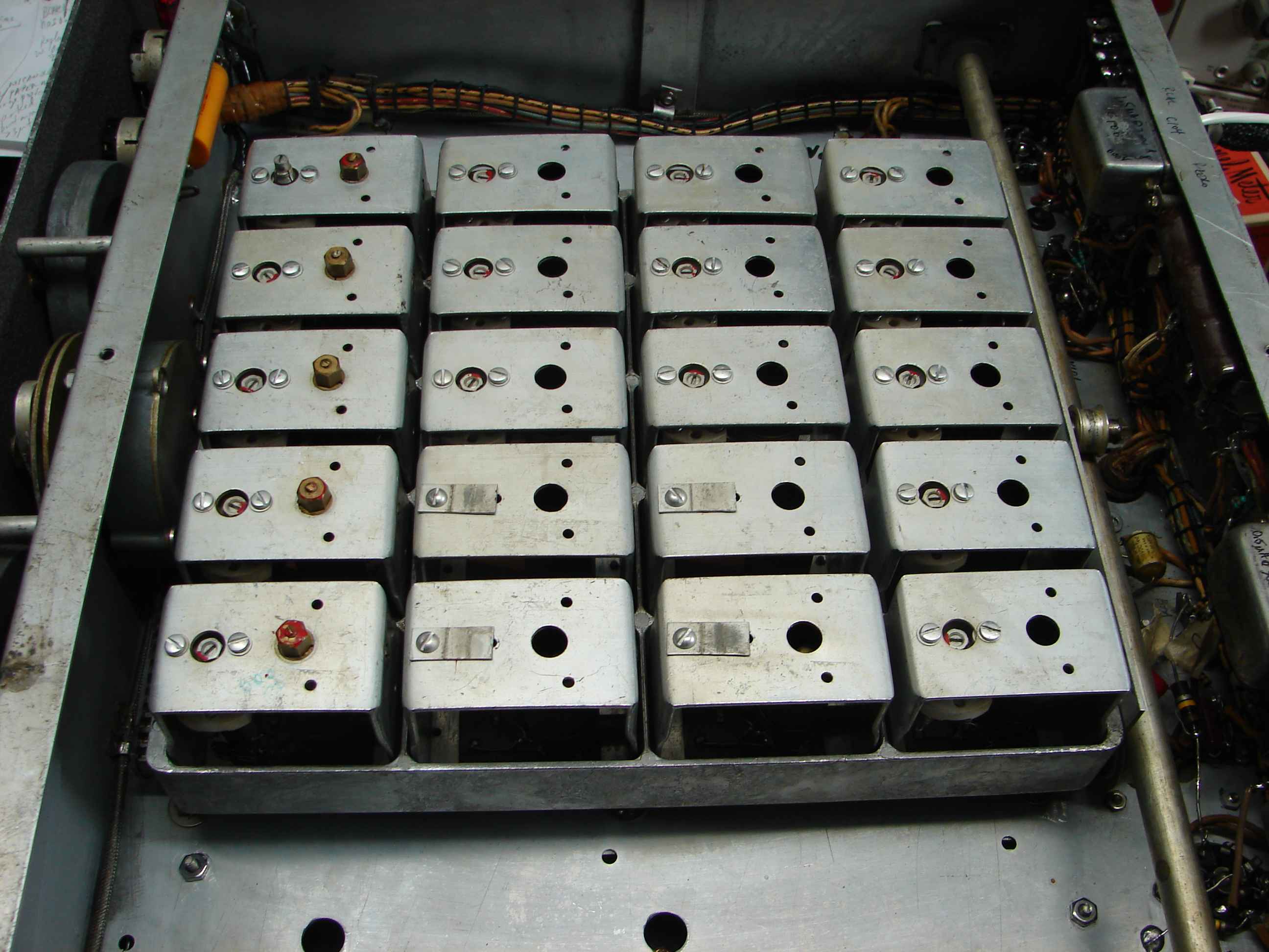
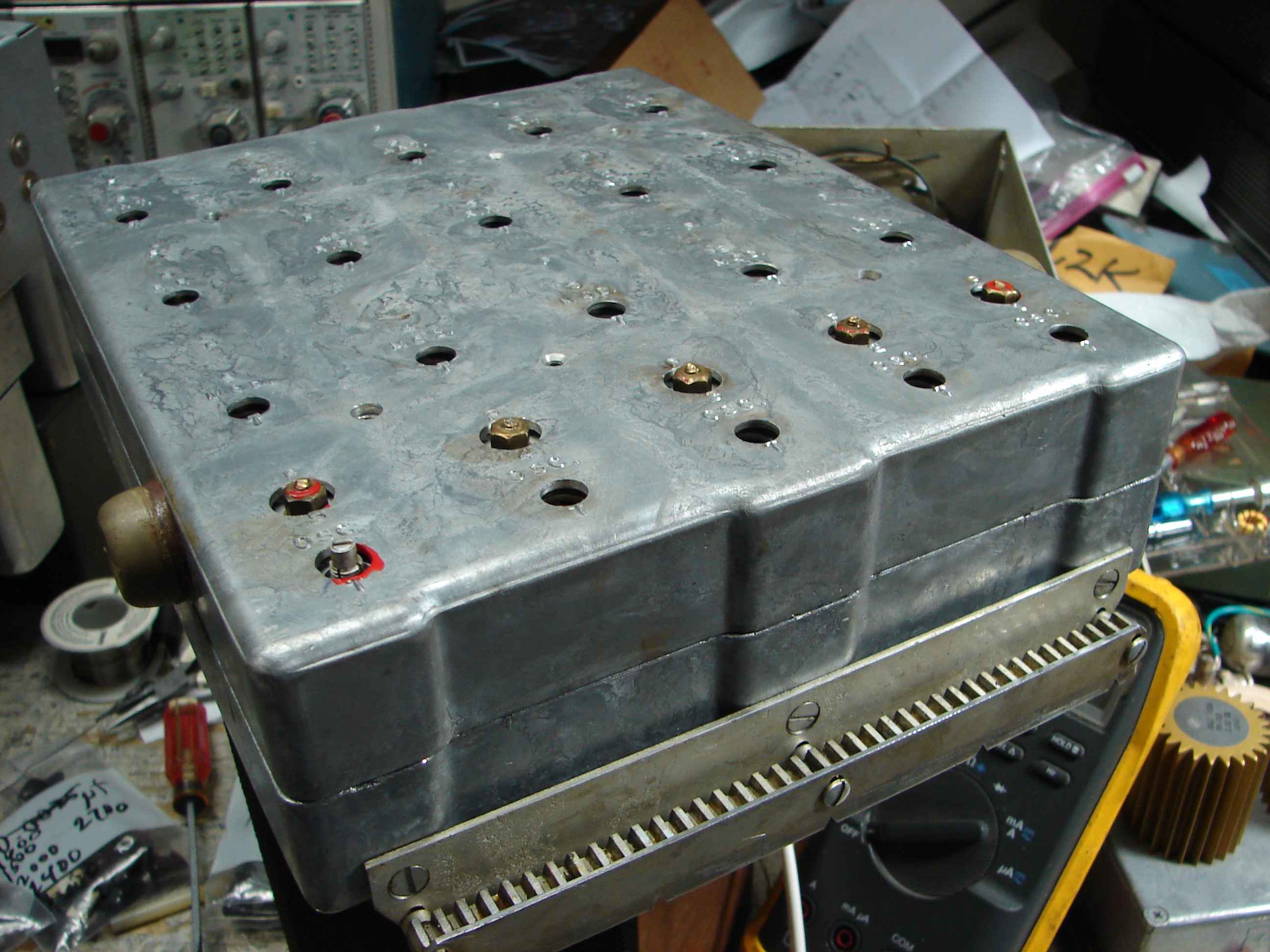
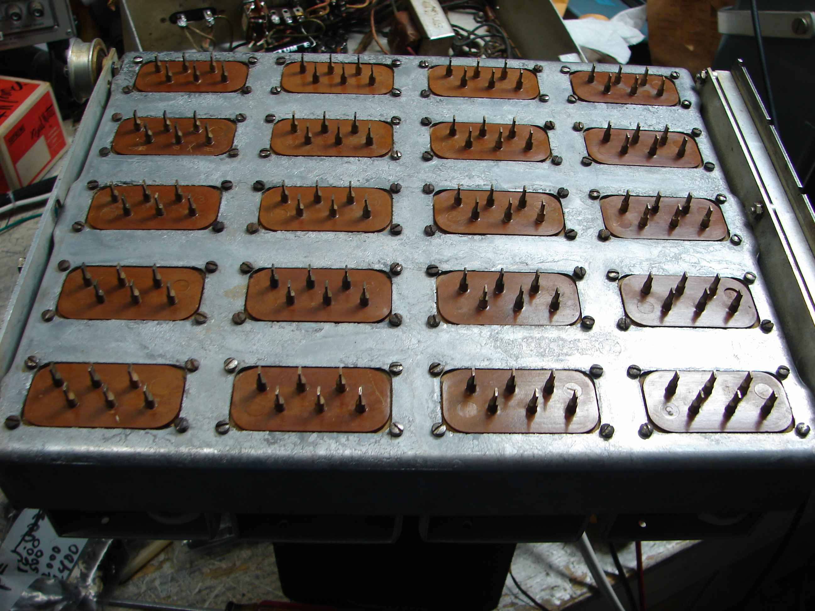
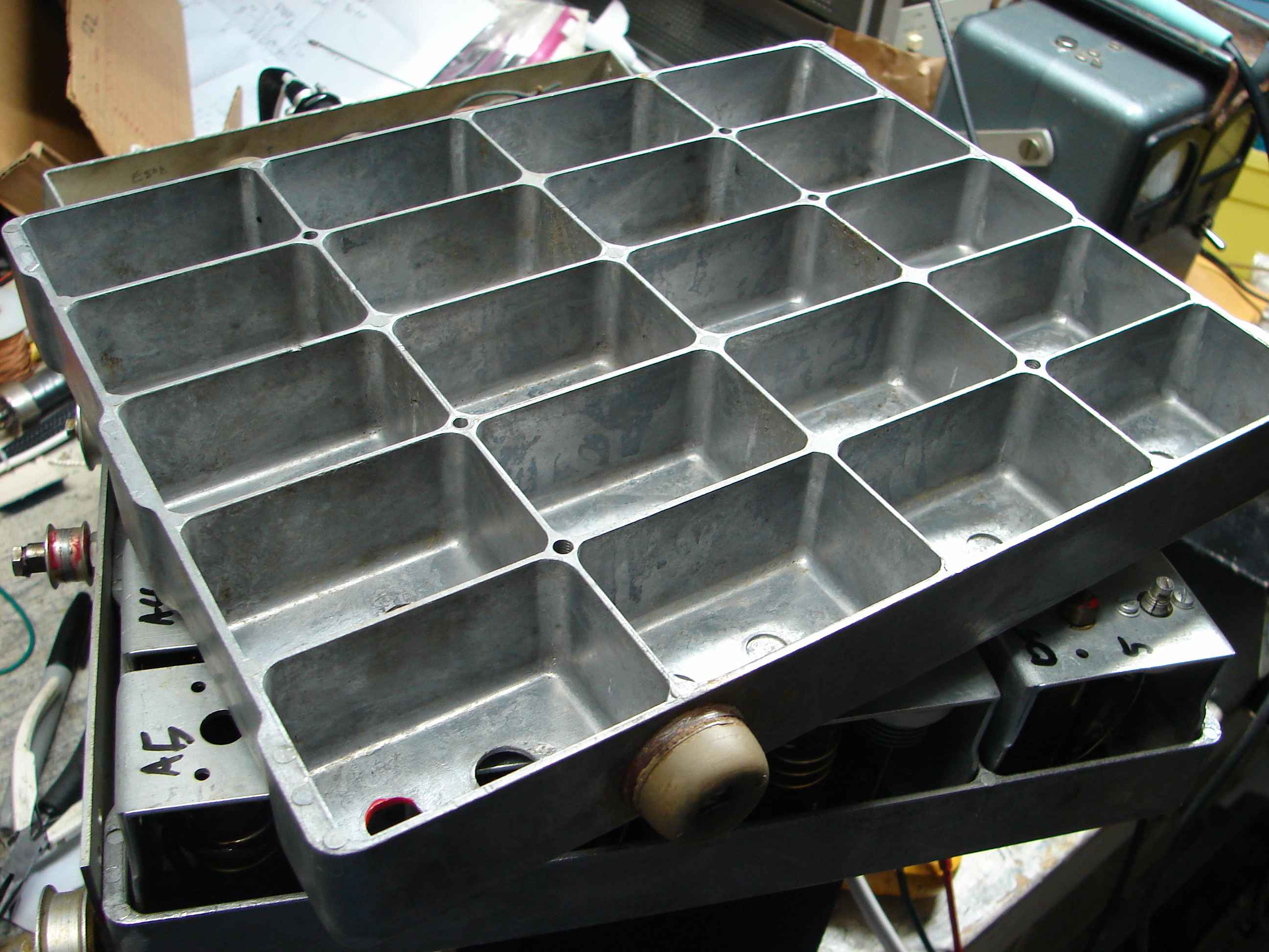
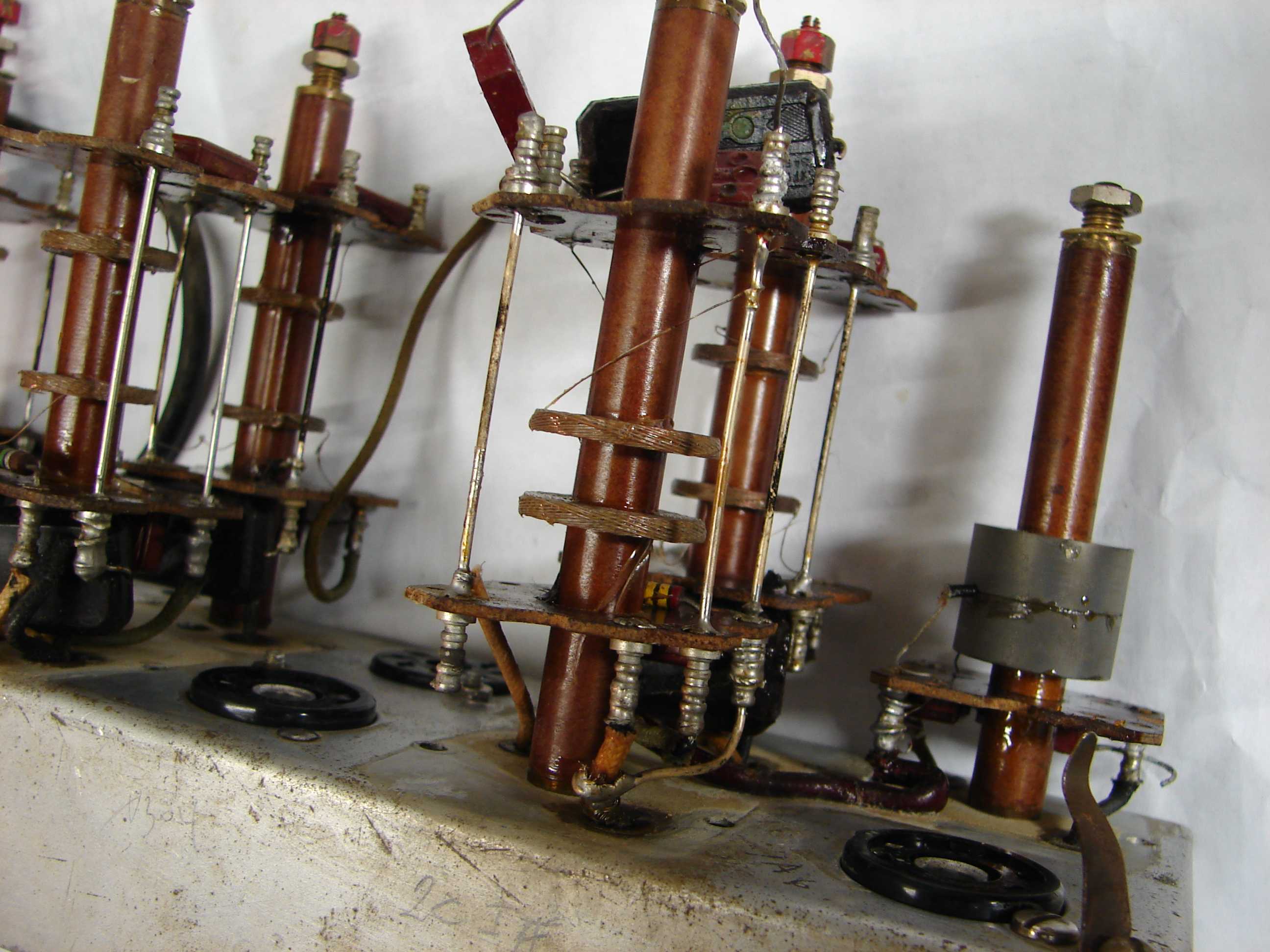
The RF section of the KP-81 features two RF stages, a pentagrid mixer, and electron-coupled Hartley local oscillator. The 500 kc crystal calibrator is switched in whenever the bandspread control is rotated to a calibration position at the high end of its scale. Mixer IF output is at 465 kc. All RF and L.O. coils are contained in individually shielded compartments within a massive, cast aluminum coil drawer located in the bottom compartment of the main chassis. The effective shielding provided maximizes image rejection, and minimizes conducted L.O. emissions at the antenna terminals. The coil drawer rides on ball bearing equipped rollers which run on a precisely machined carriage rod at the rear of the coil drawer. Each end of the carriage rod is anchored to the side of the receiver’s heavy gauge steel chassis. The front panel bandswitch control drives a gearbox which operates a rack and pinion mechanism which moves the RF coil drawer horizontally from band to band. Heavy silver plated contacts on the coil modules within the drawer engage silver plated spring fingers on the bottom of the RF subchassis. This method of bandswitching ensures that coils are connected as directly as possible to the RF circuits, with minimal lead lengths.
The input may be fed from a balanced transmission line, or from an unbalanced line, by grounding the bottom of the antenna coil primary, terminal D, to chassis ground terminal G. Antenna terminal impedance varies greatly with frequency, from a minimum of about 40 ohms to as high as 300 ohms at some frequencies, for bands 2 through 5. In most cases, impedance was less than 100 ohms, making 50 ohms the most appropriate source impedance for antennas and for alignment purposes. On band 1, 540-1700 kc, the front end is designed for high impedance operation, with the resistive part of the input impedance ranging from a maximum of 13K ohms at 550 kc, to a minimum of 1800 ohms at 1700 kc. This high impedance permits operation with a variety of electrically short antennas, including random length wires. Indeed, the receiver pulls in numerous AM broadcast stations with just a two foot length of wire for an antenna.
Sensitivity in AM mode is very good on all bands, typically 2 uV or better, although there are some areas where front end tracking errors cause dips in sensitivity. Noise figure was not measured, but is low enough to ensure the receiver is atmospheric noise limited at the upper end of band 5, with modest sized antennas.
Image rejection ranges from excellent to fair, and varies considerably with frequency. On band 1, image rejection, is at least 100 dB, referred to 1 uV input, limited mainly by L.O. phase noise, not front end selectivity. On bands 2 and 3, image rejection ranged from around 75 dB at the low end, to 55 dB at the high end, referred to 1 uV RF input. Band 4 image rejection ranged from 60 dB at 11 Mc to 40 dB at 20 Mc, and on Band 5 was a fairly consistent 40 dB from 20-30 Mc.
RF input third order intermodulation distortion was checked at a few frequencies. At 4 Mc, 3rd order IM rejection ratio was 50 dB, and at 7 Mc and 15 Mc, it was 52 dB, all referred to 1 uV RF input, with interferers at +10kc, and +20 kc. When listening in the crowded 9, 11, and 15 Mc broadcast bands on a 12 element 10-30 Mc log periodic antenna aimed at Europe from my QTH on the Atlantic coast of Florida, strong stations such as Radio Marti caused intermod problems, and inserting a 15 dB pad in the antenna feedline was beneficial. This would not likely be necessary using smaller antennas. AVC range was adequate for receiving the strongest broadcast stations without distortion.
Adjacent channel rejection checked at +10 kc was 77 dB.
These measurements indicate the KP-81 is a good performer, similar to the better receivers of the 1940s.
The KP-81 IF signal path features nine tuned stages utilizing specially designed high Q permeability-tuned IF transformers, and three IF amplifiers, plus a crystal filter, to obtain a high degree of selectivity. Pierson used the somewhat unorthodox technique of capacitive bottom-coupling of adjacent double-tuned IF transformers. A maximum selectivity of 4 kc is set by the aggregate effect of these tuned stages, and this can be reduced to a minimum of about 500 cps through the use of the crystal filter. Unlike some other receivers of its day, a wideband IF setting for high fidelity reception was not provided. As the nameplate indicates, the KP-81 was designed as a communications receiver. Audio quality is nonetheless good, and the high selectivity minimizes the 5 kc beats which plague present-day HF broadcast reception. Proper sweep alignment of the IF will provide a good, symmetrical IF response, with reasonably flat group delay. IF selectivity is very satisfactory for AM operation in the crowded 75 meter band, and the noise silencer adds little audio distortion. CW reception with the crystal filter in series mode at minimum bandwidth is very satisfactory, without objectionable ringing, although one might wish for higher a BFO injection level. The post detection, switchable highpass/lowpass audio filter allows several audio response settings, from extended low frequency response to a narrow bandpass response for CW reception.
Despite the hyperbole in its promotional literature and owner’s manual, most of the circuitry of the KP-81 is fairly conventional, and not radically different in concept from other high quality general coverage receivers of its era. An exception to this is its noise silencer circuit, a unique design which was significantly more sophisticated than that of contemporary receivers, and which is worth examining in detail. The circuit dates back to Pierson’s 1937 efforts at improving upon the well-known Lamb Noise Silencer, patented by James J. Lamb that same year. Associated with Pierson’s work are some interesting historical footnotes, also worth recounting.
Karl Pierson, then chief engineer of Pierson-DeLane, Inc., had been heavily involved in coordinating amateur radio relay operations in support of Amelia Earhart’s first 1937 attempt at an around-the-world flight. Using a modified Pierson-DeLane PR-15 receiver containing an early version of the silencer circuit, Pierson claimed to have received distress signals from Earhart after she disappeared on her fateful flight from Lae, New Guinea to Howland Island. Pierson attributed this feat (strongly disputed by some) to the remarkable properties of his noise silencer circuit.
By 1941, Pierson claimed to have perfected the design, and had attracted the interest of the U.S. Army Signal Corps Laboratories at Ft. Monmouth, NJ, who were interested in its possible use in military HF receivers. The Signal Corps purchased several evaluation receivers featuring the Pierson silencer. Pierson anticipated a contract to supply production receivers to the Signal Corps, but it is not clear just what these receivers would have been, or whether anything beyond the prototypes was ever supplied.
Pierson also managed to secure the endorsement of Lee DeForest, who, in a Dec. 4, 1941 AP news story, praised the circuit saying, "Pierson has accomplished what no other radio engineer working with amplitude modulation has succeeded in doing. He employs special silencers which possess the unique quality of cutting out or reducing in their intensity to an astounding degree all sorts of interference. It undoubtedly will prove an important factor in military radio communication." Later, in a second AP article of March 19, 1942, DeForest stated that the circuit "brings in programs and signals through static which even the most advanced of modern receivers fail to make intelligible. DeForest continued, "Tests showed the receiver can pick up messages through interference noise four times the intensity of the signals themselves, exceeding in this respect frequency modulation sets." One wonders if, in saying this, DeForest was taking a dig at his old rival and wideband FM inventor, E.H. Armstrong.
In these articles, Pierson himself revealed no details of the silencer’s operation, except to say that "It more or less contradicts accepted theory and practice, which may be the reason it had not been discovered before. One of its functions, which is contrary to what one might expect, is that the greater the noise, the better it is eliminated, and further, the weaker the signal, the greater is the noise reduction."
With all this hype, the question naturally arises as to what kind of circuit the Pierson Noise Silencer actually is, and how well it really functions. Examination of the schematics clearly shows that Pierson’s design is an extension of the classical Lamb technique. In a typical implementation of the Lamb circuit, the receiver’s IF signal is applied to a pentode noise amplifier which in turn drives a diode detector which conducts upon receiving large-amplitude IF noise impulses. The detector conduction threshold is manually set by a potentiometer which sets the noise amplifier cathode bias. The detector output is a negative-going blanking pulse, fed to the first grid of a pentagrid converter tube used as a gated IF amplifier. The IF signal, applied to the second grid, is amplified by the pentagrid tube, which is brought into cutoff for the duration of the grid #1 blanking pulse. The IF signal is thereby gated off for the duration of a noise impulse, suppressing noise in the recovered audio.
Pierson improved upon the Lamb circuit by eliminating the manual noise threshold control, which needs frequent adjustment according to signal and noise conditions, and providing an auto-threshold circuit, which continually optimizes the blanking threshold as signal conditions vary, based on receiver AVC voltage. The Silencer is located at a point of moderate selectivity, and ahead of the crystal filter, thus greatly reducing ringing of the IF tuned circuits and crystal filter caused by impulse noise.
When properly aligned, the Pierson Silencer does work surprisingly well, greatly reducing power line noise, automobile ignition noise, electric fence impulses, and lightning static crashes, without need for manual adjustments of any kind. Distortion of amplitude modulated signals is negligible with the silencer switch in the FONE position, but noticeable in the CW position. The degree of noise suppression depends to some extend on the nature of the noise, and is most effective on high-amplitude, short duration impulse noise. High amplitude, very "spiky" power line noise is usually essentially eliminated. Pierson’s comment, that "the greater the noise, the better it is eliminated", seems to be accurate. His statement "the weaker the signal, the greater is the noise reduction" is also true, although another way of stating this might be, "the greater the signal, the less is the noise reduction." And this actually seems to be the case, as the AVC control action of the system does seem to somewhat reduce noise blanking effectiveness. For example, if under noisy, no-signal conditions, a lightning noise burst occurs, developing AVC action, the impulse noise momentarily increases until the AVC voltage decays back to the nominal value. Similarly, when tuning in an AM signal under noisy conditions, turning the noise blanker on or off makes much less difference than if the AM carrier were not present at all. This a minor drawbacks however. Somewhat more significant is the tendency of the silencer to alter the IF passband response, when it is switched in. The reason for this will be discussed in more detail later. On the whole, the Pierson noise silencer is effective, and possibly the best found in 1940s vintage receivers.
Antenna signals are applied to the primary of the antenna coil, which is brought out to antenna terminals A and D. The secondary of the antenna coil is capacitively coupled to the grid of common-cathode 1st RF amplifier V202 through a 47 ohm parasitic suppression resistor. AVC voltage developed in the IF section is fed to V202 through a RF decoupling network consisting of R204, C231, R215, and C219. This network also establishes the RF AVC time constant. A positive bias voltage applied to the AVC network through voltage divider R205/R219, and R220, sets the RF AVC delay threshold. N201 and N202 are 0.1W neon lamps which protect the RF circuitry from damage from excessive RF input levels. Second RF amplifier V203 functions in similar manner, but receives AVC voltage from the top of C219.
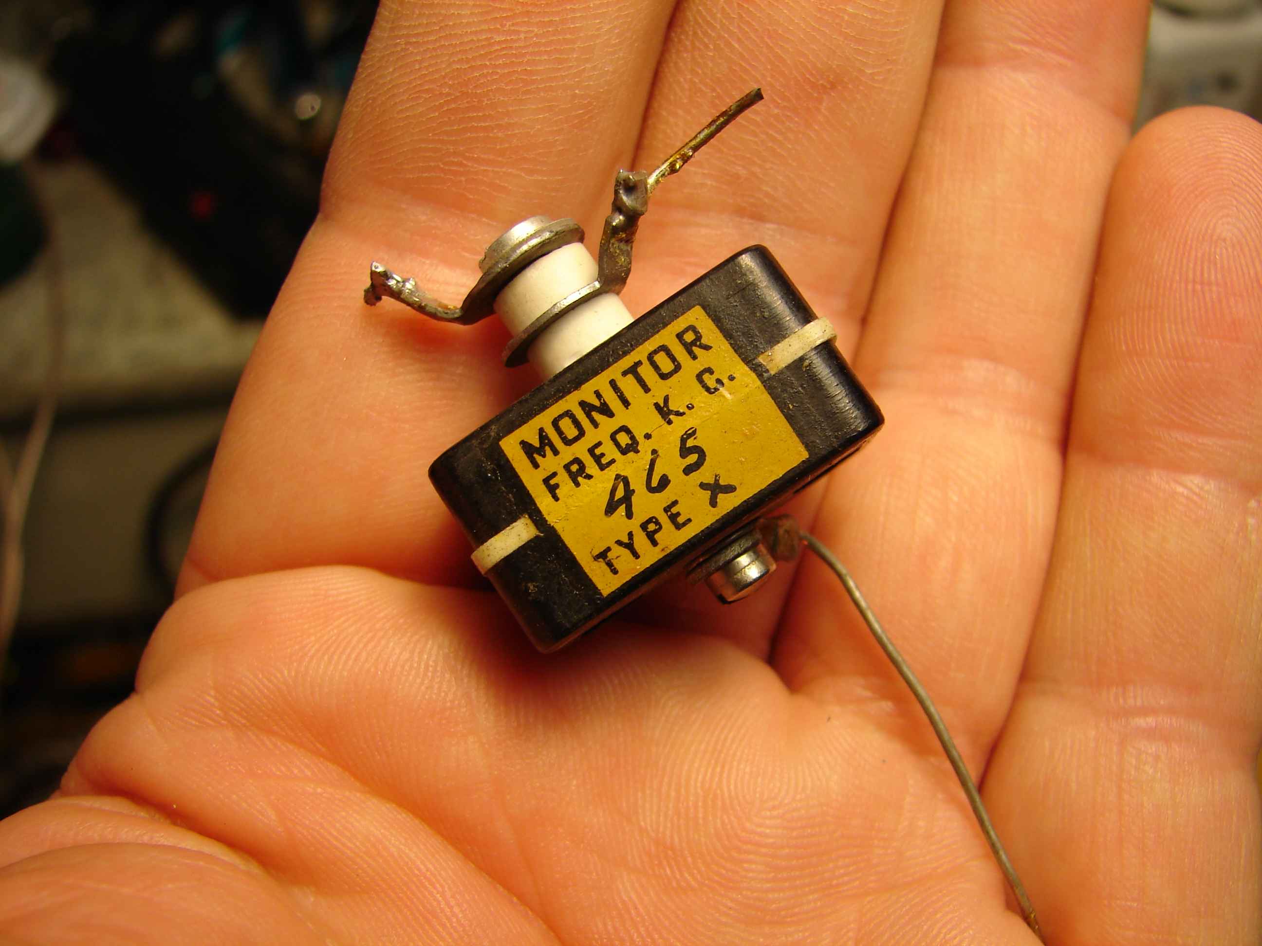
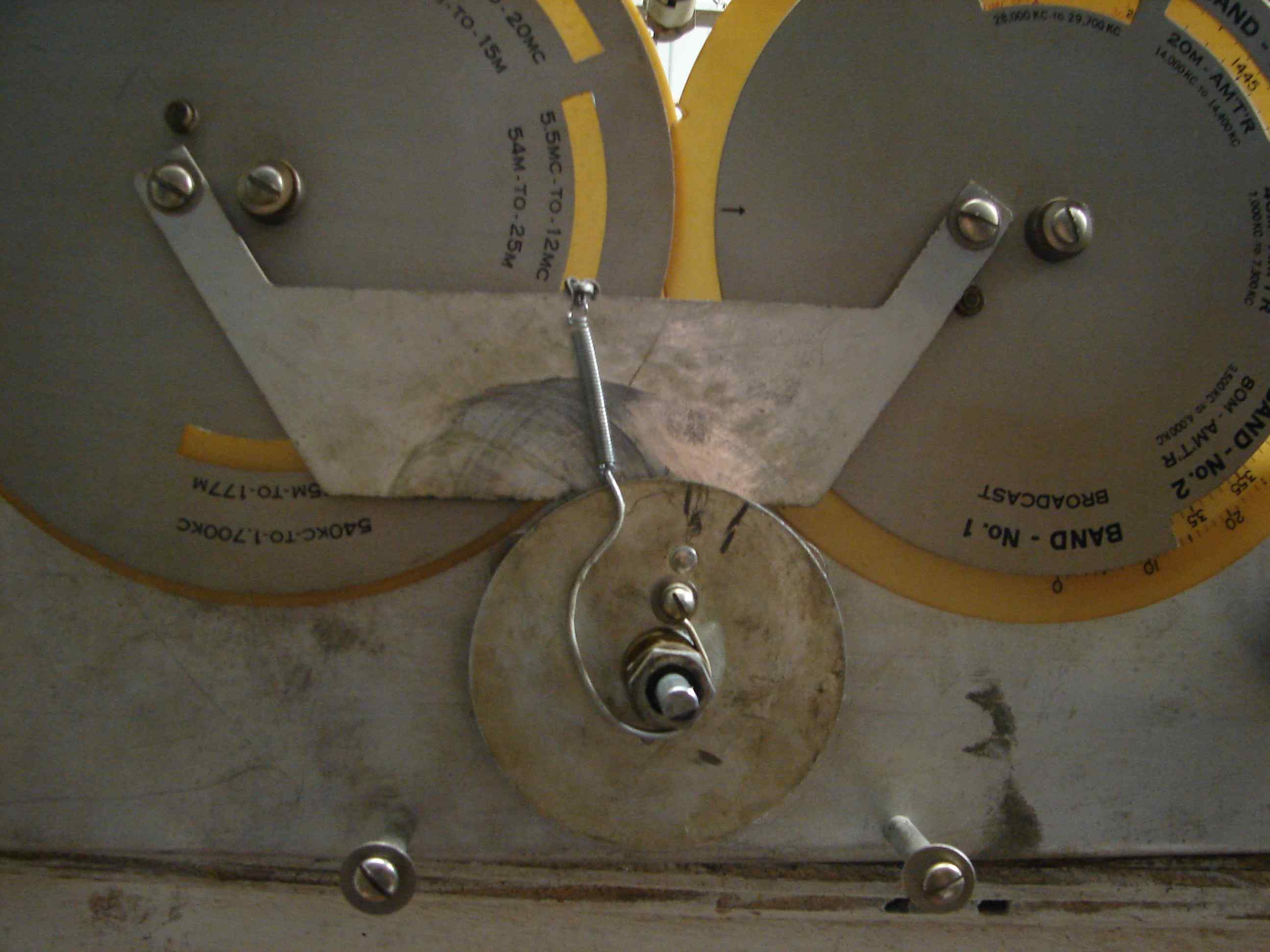
500 kc crystal calibrator oscillator V201 injects harmonic calibration markers into the input circuit of the V202. The calibrator utilizes a 500 kc FT-241A crystal, a war surplus type originally used as the "Channel 70" (27.0 Mc) crystal in the military BC-604 FM transmitter. When the bandspread dial is set to the red "XTAL CAL ON" marking, an actuator arm attached to the bandspread tuning capacitor rotor actuates microswitch S201, shorting the antenna input, and activating the calibrate oscillator.
The tuned output of 2nd RF amplifier V203 is fed to grid #4 of pentagrid mixer tube V204. Local oscillator drive is supplied to V204 grid #1 by V205, an electron-coupled Hartley oscillator.
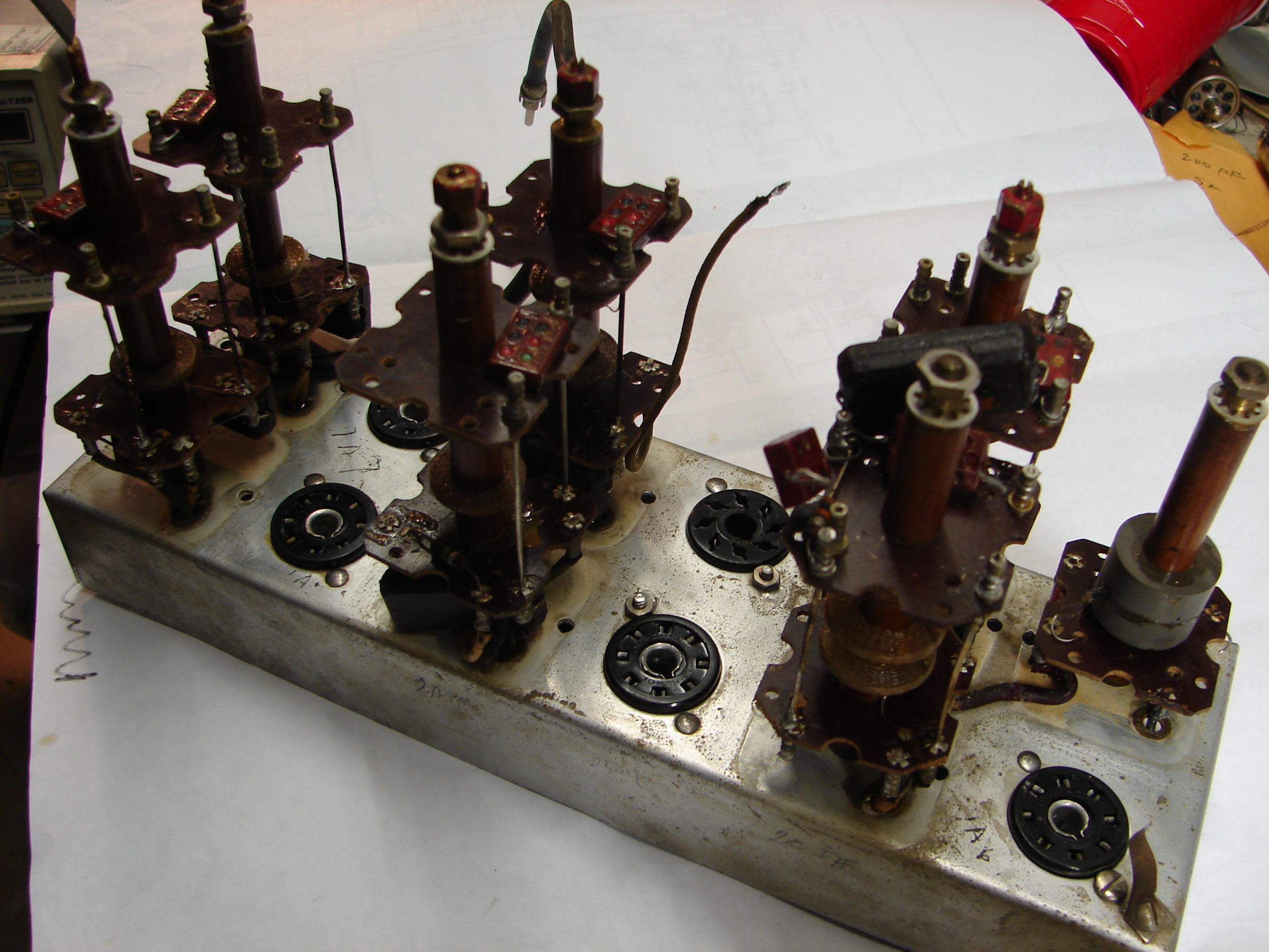
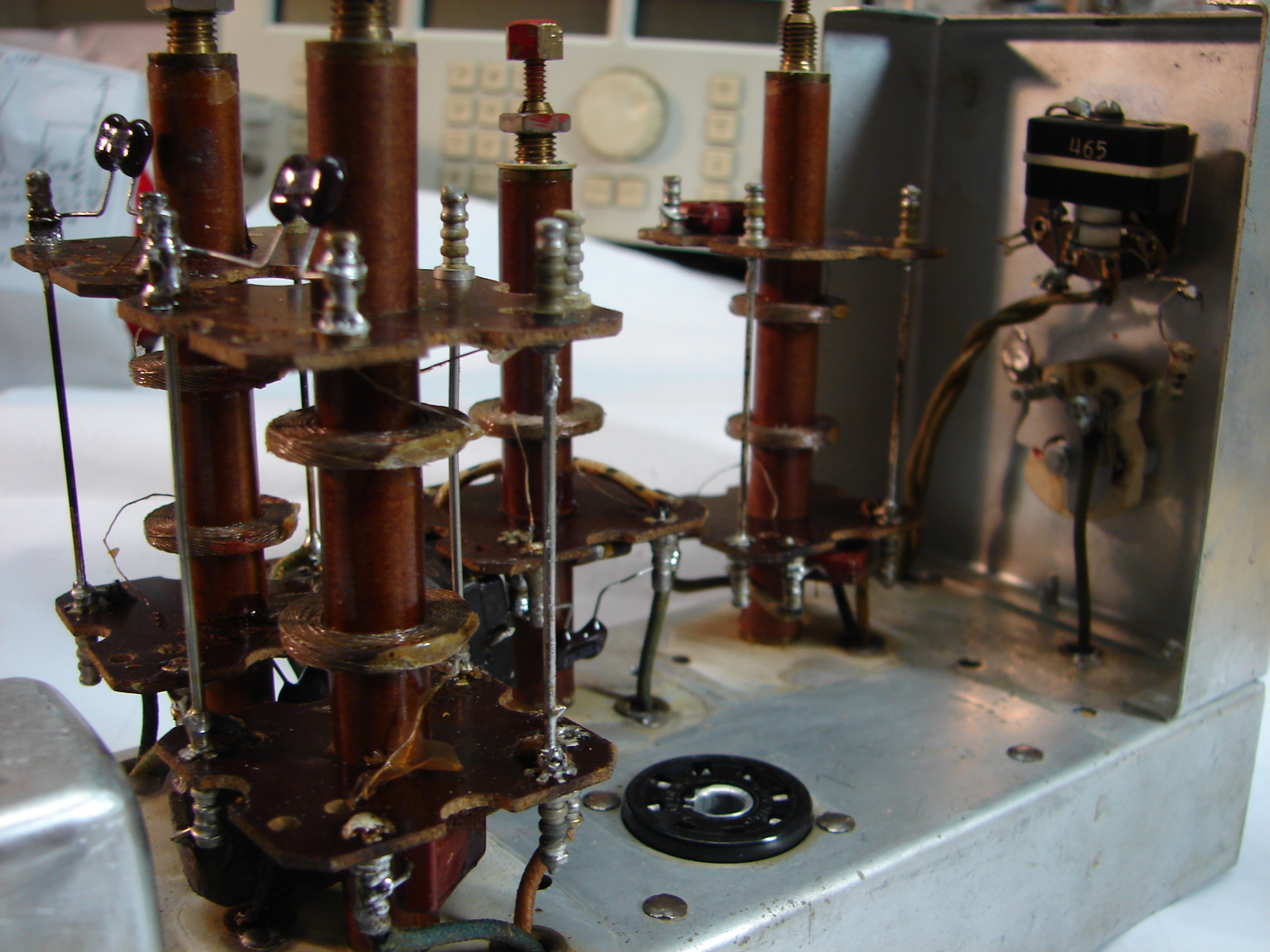
IF output from the RF chassis is fed to the primary of double-tuned IF transformer 1A via a section of coaxial cable to P201. B+ for RF mixer tube V204 is routed to this cable via R314 and the 1A primary coil. The secondary of 1A is bottom coupled to the primary of double-tuned IF transformer 1B by bottom coupling capacitor C325, which establishes the coupling coefficient between the two IF transformers. IF signal and IF AVC voltage is fed to the grid of 1st IF amplifier V301 via transformer 1B secondary. Output from V301 is developed across the primary of IF transformer 2A. 2A secondary, however, is not part of the main IF signal path, but couples a sample of the IF signal to IF noise amplifier V304, part of the Noise Silencer circuit. The primary of transformer 2A is bottom coupled to the primary of IF transformer 2B by C322. 2A primary together with 2B primary and secondary, form a triple-tuned circuit, and 2B secondary feeds the IF signal to 2ndIF amplifier V302, a pentagrid tube. V302 plate output is developed across L309 and C309, the primary circuit of IF transformer 3A. 3Asecondary output is bottom coupled by C311 to the primary of IF transformer 3B, on the #2 IF chassis.
A sample of the IF signal is taken from the secondary of IF transformer 2A, and applied to the grid of pentode V304, the noise IF amplifier. When Silencer switch S301 is set to the "FONE" position, the gain of V304 is controlled by the receiver’s AVC voltage, applied to its grid via R312 in the 2A secondary circuit. Noise IF output is taken at the secondary of noise IF transformer 2C, and fed to one anode of diode V303. A negative bias is applied to V303 anode from the receiver AVC bus via R308 and L311 within the 465 kc IF rejection filter 2D. The negative bias on V303 anode therefore is proportional to received signal strength, and serves as a variable blanking threshold voltage. IF noise impulses which overcome the negative blanking threshold bias cause V303 to conduct, and a detected noise pulse is developed across R306 to ground. This serves as the blanking pulse, and is applied to grids 2 and 3 of pentagrid IF amplifier tube V302 through L311 in the rejection filter, and via C331 and C330, respectively. Note that V302 grid 2 and 4 are internally connected within the tube. The rejection filter prevents IF signal and noise voltage components present at R306 from being amplified by V302, while permitting blanking pulses to pass to V302. The IF signal, riding on the AVC voltage, is fed from the secondary of double-tuned IF transformer 2B to V302 grid 1 for amplification. AVC voltage is fed to the grid of pentode V305 through an RC network consisting of R301 and C301 which filters out the blanking pulses riding on the AVC voltage. V305 functions as an inverting DC amplifier which provides a positive voltage to V302 grids 2 and 4 which varies inversely with received signal strength. V305 anode voltage is derived from the highest voltage tap on voltage divider resistor R114 on the main chassis, via V305 plate resistor R309. V305 screen is fixed at the same potential as the top of R309. The cathode of V302, together with grids 1 and 2 therefore function as a triode amplifier, with grid 1 serving as control grid, and grid 2 serving as anode. IF output from V302 is coupled to the primary of IF transformer 3A in the V302 plate circuit. The positive voltage at "anode" grid 2 goes somewhat negative during each blanking pulse, and the nominal value of this "anode" voltage and the negative grid 1 bias derived from the AVC bus track one another as a function of signal strength. The second section of V303 clamps V302 grid 3 at ground potential. The tracking of the blanking threshold bias voltage and "anode" grid 2 voltage ensures that V302 functions normally as an IF amplifier, but will be reliably cut off during each blanking pulse, over a wide range of both desired signal amplitude and impulse noise amplitude, with minimal audio distortion.
When Silencer switch S301 is set to the CW position, V305 grid is grounded, the tube is in saturation, and V302 grid 2 voltage is very low. Typically, in CW mode, AVC is switched off, and the RF gain control is varied manually as a function of signal level. Therefore, with the silencer in CW mode, V302 "anode" grid 2 voltage is fixed at a low value, and blanking action depends on the RF gain setting in manual gain mode, or with AVC action in AVC mode. The AVC-derived blanking threshold in "FONE" means that noise blanking is at a maximum under zero or weak signal conditions, and is reduced on moderate to strong signals. This appears to have been a design compromise between blanking aggressiveness and audio distortion on AM signals. Perhaps the rationale was that impulse noise is less disturbing as carrier level increases, and audio distortion then becomes the dominant consideration. The CW position essentially eliminates the influence of signal strength on noise blanking, and provides more "aggressive" blanking at the expense of increased audio distortion, which is tolerable in CW operation. In AM mode with very noisy conditions, the CW setting of the silencer may be the best choice.
There is actually a secondary, somewhat sneaky reason for providing a separate CW setting of the silencer—eliminating the effect on blanking action of BFO leakage into the IF. BFO leakage is high enough that some AVC action is developed when the BFO is on. This reduces blanking action somewhat in the FONE mode, and switching to the CW setting of the silencer eliminates this problem.
A potential problem with the silencer circuit is that it introduces a potential "sneak path" from the noise amplifier output to the input of the 2nd IF amplifier stage when the silencer is switched in. If receiver gain with the silencer on or off is unequal, the receiver noise level may actually increase when the silencer is switched on. Balancing receiver gain with the Silencer on or off is necessary during alignment to prevent this.
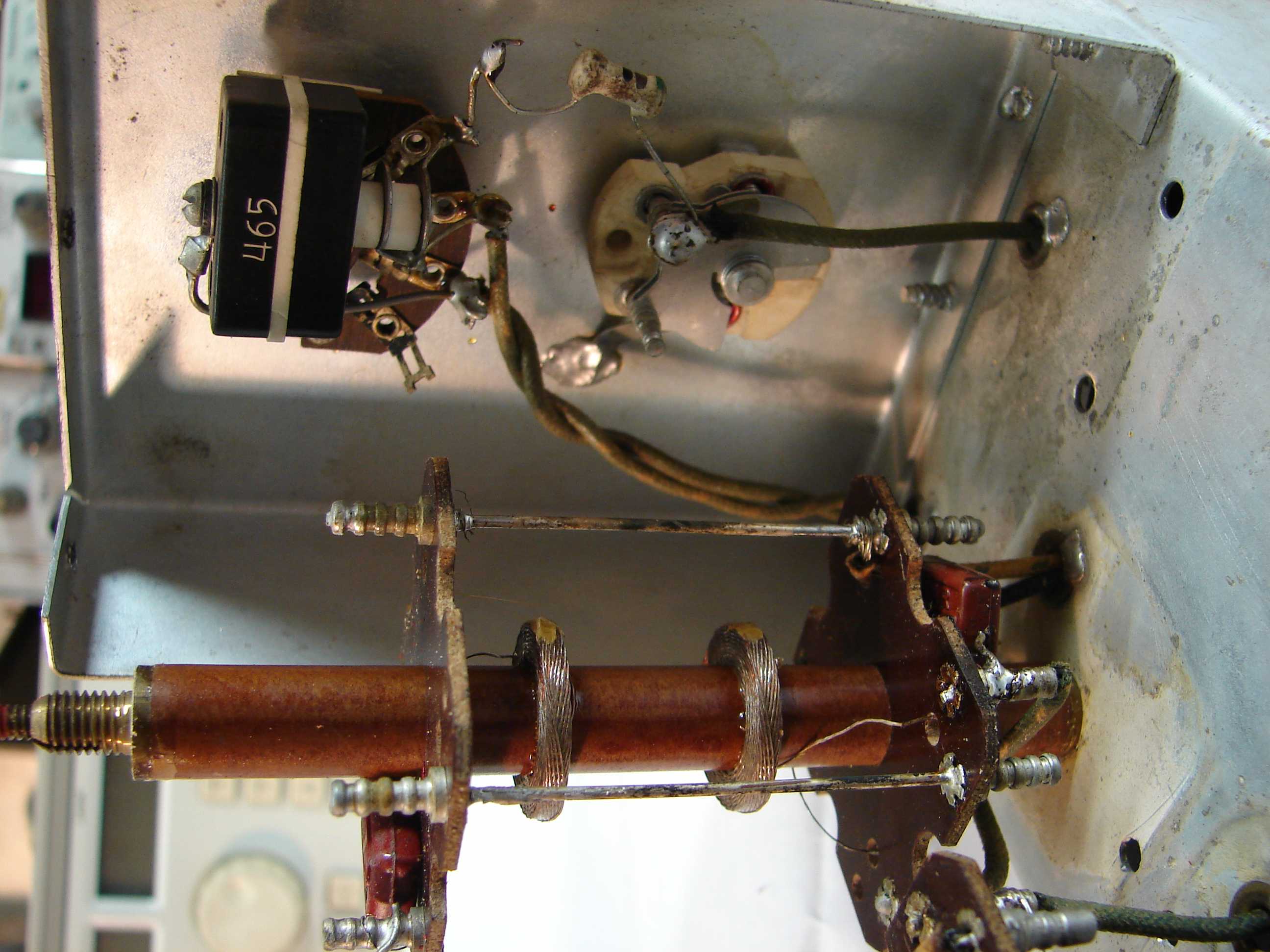
Output of IF transformer 3A in the #1 IF chassis is bottom coupled to the primary of IF transformer 3B, by the parallel combination of C311 on the #1 IF chassis, and C402 (see parts list) at the bottom of 3B primary. Transformer 3B couples IF signal to the crystal filter. The crystal filter may be operated in typical series resonant mode with a front panel phasing control providing variable bandwidth, or in parallel (antiresonant) mode as an IF notch filter.
3rd IF amplifier V401 drives two more double-tuned, bottom-coupled IF transformers, 4A, and 4B, with 4B secondary feeding the detector stage, V402.
V402 functions as an "infinite impedance" detector. A large cathode resistor, R405, places a large cathode bias on V402, keeping it at or near cutoff. The positive-going portion of the IF signal drives V402 into conduction, and detected audio is developed across the cathode resistor and cathode bypass capacitor C409, which filters out the IF signal. Since V402 functions essentially as a rectifying cathode follower, it presents a high load impedance to the last IF transformer, preserving tuned circuit Q.
The KP-81 features a carrier level meter calibrated in “R”
units above 1 microvolt with a semi-logarithmic scale.
“R1” therefore represents approximately 0 dBuV, with each additional
R unit representing an increase in signal strength of 6 dB.
Above “R9” or +48 dBuV, two “+” signs indicate two additional 12
dB increments, with an abrupt and undefined increase in slope above this.
On this scale, the conventional “S9” signal strength of 50 uV (+34
dBuV) appears just under R7.
BFO V403 is an electron-coupled Hartley oscillator which drives the plate of detector V402 via a capacitive voltage divider. The BFO signal at the plate of V402 modulates its plate current and thus the IF signal, producing an audio frequency beat at V402 cathode on CW signals.
The KP-81 features a simple and reasonably effective AVC-derived squelch circuit. V102 serves as the squelch control tube. The cathode resistor of 1st audio amplifier V103 connects to the cathode of squelch tube V102, and to ground through the wiper arm of squelch control potentiometer R108. When the front panel SQUELCH control is rotated to the OFF position, squelch switch S103 grounds the bottom end of R103 and V102 cathode, and shorts across the upper portion of R108. V103 then receives nominal cathode bias, and functions normally. With the SQUELCH control just set to ON, R103 is lifted from ground, and the short across R108 is removed, and the cathode bias on V103 is a result of the combination of the cathode currents of both V102 and V103 flowing in the series combination of R103 and squelch potentiometer R108. The grid voltage of V102 is a sample of the receiver AVC voltage from a voltage divider consisting of R104 and R105. Under no-signal conditions, AVC voltage is at its least negative value, and V102 conducts heavily. However, since R108 is at its minimum value, essentially zero, V103 still conducts normally. If the squelch control is steadily advanced (R108 increasing in resistance from minimum), the voltage across R108 increases, increasing the cathode bias on V103 until at some point the it is sufficient to cut off V103, and the audio is squelched. The squelch threshold is now set, and increasing received signal strength causes the AVC voltage to go more negative. V102 conducts less heavily, the voltage drop across R108 decreases, and the cathode bias on V103 decreases. When received signal strength is sufficiently high, cathode bias drops sufficiently to bias V103 into conduction and the receiver is unsquelched.
WARNING: Before applying power to the receiver, make certain the ground straps on the cable interconnecting the power supply/audio amplifier unit and the receiver are securely connected to their chassis ground terminals at both ends. The power supply/audio amplifier has no chassis ground connection to any pin on the interconnecting cable. The chassis ground interconnection is solely through the cable outer shield. If the ground straps are not connected to their respective chassis ground terminals, the power supply/audio amplifier chassis will float at high voltage, the receiver will not function, and a potential difference of over 300V will exist between the two chassis, with low source impedance. This astonishing design oversight can result in electrocution.
The KP-81 requires some special handling precautions due to its unusual design and its large size and weight. The receiver contains a large, heavy, cast aluminum RF coil drawer mounted underneath the chassis, which is moved horizontally on a carriage by the bandswitch gear box. A spring-loaded ball detent mechanism locks the drawer in the correct position at each band setting. Unfortunately, the detent mechanism is not always sufficient to hold the coil drawer in place if the receiver is placed on its side for servicing or inspection. It doesn’t take much bumping around on the bench to disengage the detent, causing the coil drawer to "crash" under the force of gravity. This can cause serious damage to the coil contact fingers and to the bandswitch shutter drive mechanism and tensioner spring. Always set the bandswitch to place the coil drawer in its "lowest" position--either Band 1 or Band 5, depending on which side the receiver is to be placed. When it’s safely on the bench, the bandswitch may be set as needed. Even then, it’s a good idea to support the coil drawer by some means.
The KP-81 RF coil drawer must be locked in place prior to shipment to prevent the coil drawer from thrashing around and damaging the contact fingers. Place the receiver on its side (following above precautions), and set the bandswitch to Band 3. Insert two 8-32 screws through the openings in the bottom cover plate and into the two threaded holes in the coil drawer. Tighten the screws securely. If you’re having a receiver shipped to you, be absolutely sure the seller understands and complies with this requirement. Failure to do so can really trash the receiver.
Tuning slug lead screws of several of the IF transformers can be broken by accidental contact with the front upper lip of the cabinet while withdrawing the receiver chassis from its cabinet. To avoid damage, the chassis must be carefully maneuvered during removal to ensure that the tuning slug screws all pass through slots in the cabinet upper lip provided for this purpose.
Inspecting a KP-81 for condition differs little from that of any other receiver of its time period, but there are a few inspection items peculiar to this set which are worth looking out for.
Inspect the main tuning and bandspread plastic dial cards for chips or other damage around their edges. The KP-81 tuning shafts engage and drive the edges of the dial cards, and chips or breaks in the card edges can ruin the tuning mechanism. Repairing chewed up dial cards would be a major ordeal.
Invert the receiver on the bench, being careful to support the rear of the chassis to prevent the IF transformer tuning screws from contacting the bench surface. A wooden block of the appropriate height placed under the audio interstage transformer at the rear of the chassis will do the trick. Slowly rotate the bandswitch, listening for any telltale sounds of misaligned contacts. If all appears well, set the receiver to either Band 1 or Band 5. The
condition and alignment of the RF coil contacts can then be inspected by looking underneath the coil drawer. A mechanic’s mirror is helpful here. Look for bent, broken, or otherwise damaged contact fingers on the bottom of the RF subchassis, and bent or broken pins on the coil modules in the coil drawer.
The front panel bandswitch control drives a gearbox which operates a rack and pinion which moves the RF coil drawer from band to band. Over time, the gearboxes wear, and develop significant looseness or "play. Few KP-81 gear boxes remain tight today, and you can expect 20 degrees or so of play. This is fairly common, and not generally a serious problem.
The KP-81 features a unique optical dial illumination system in which the dial fiducial is projected onto the back of each dial card by a lamp positioned behind a vertical cylindrical glass lens. Light passing through the lens projects an illuminated line on the dial card, which looks nifty and has the added benefit of eliminating parallax error. Unfortunately, the cylindrical glass lenses are easily broken off, and it’s not uncommon to find one or both missing.
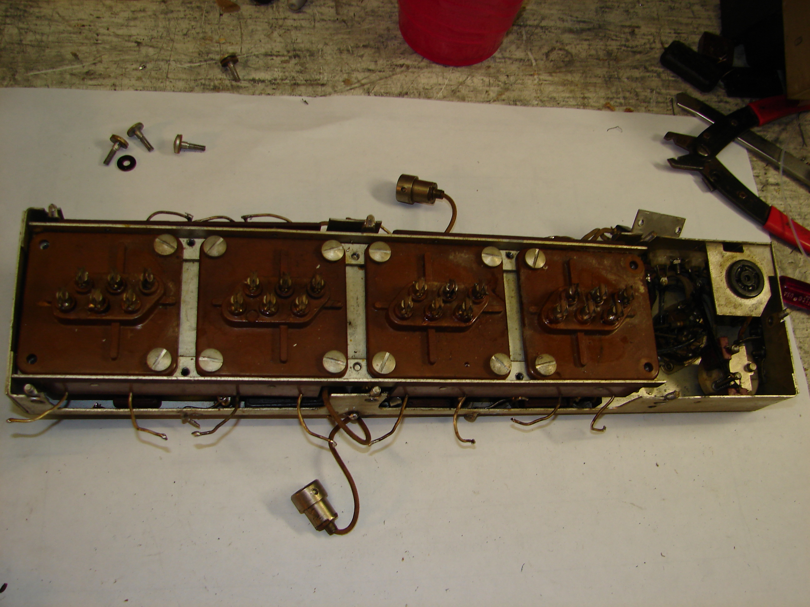
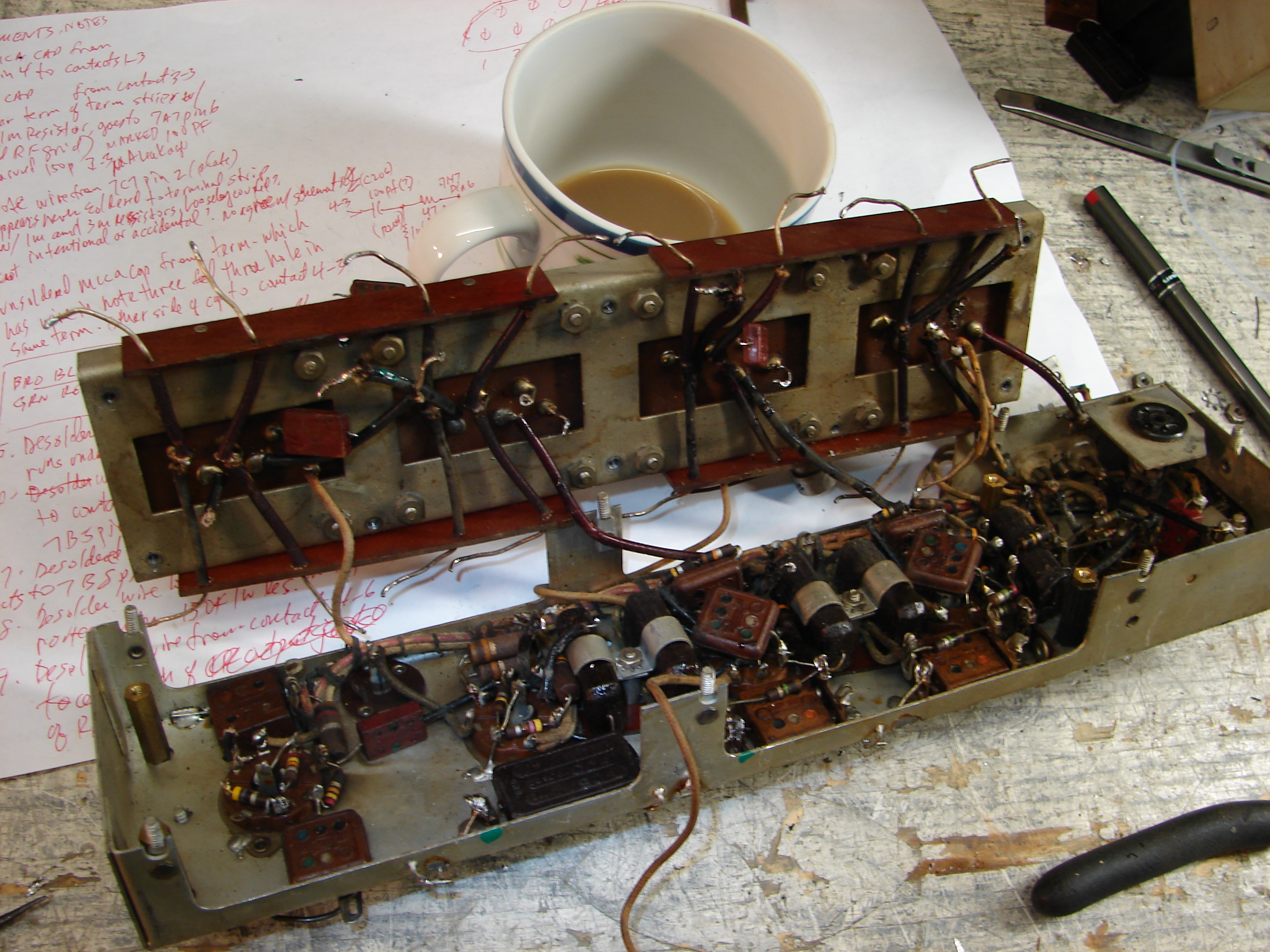
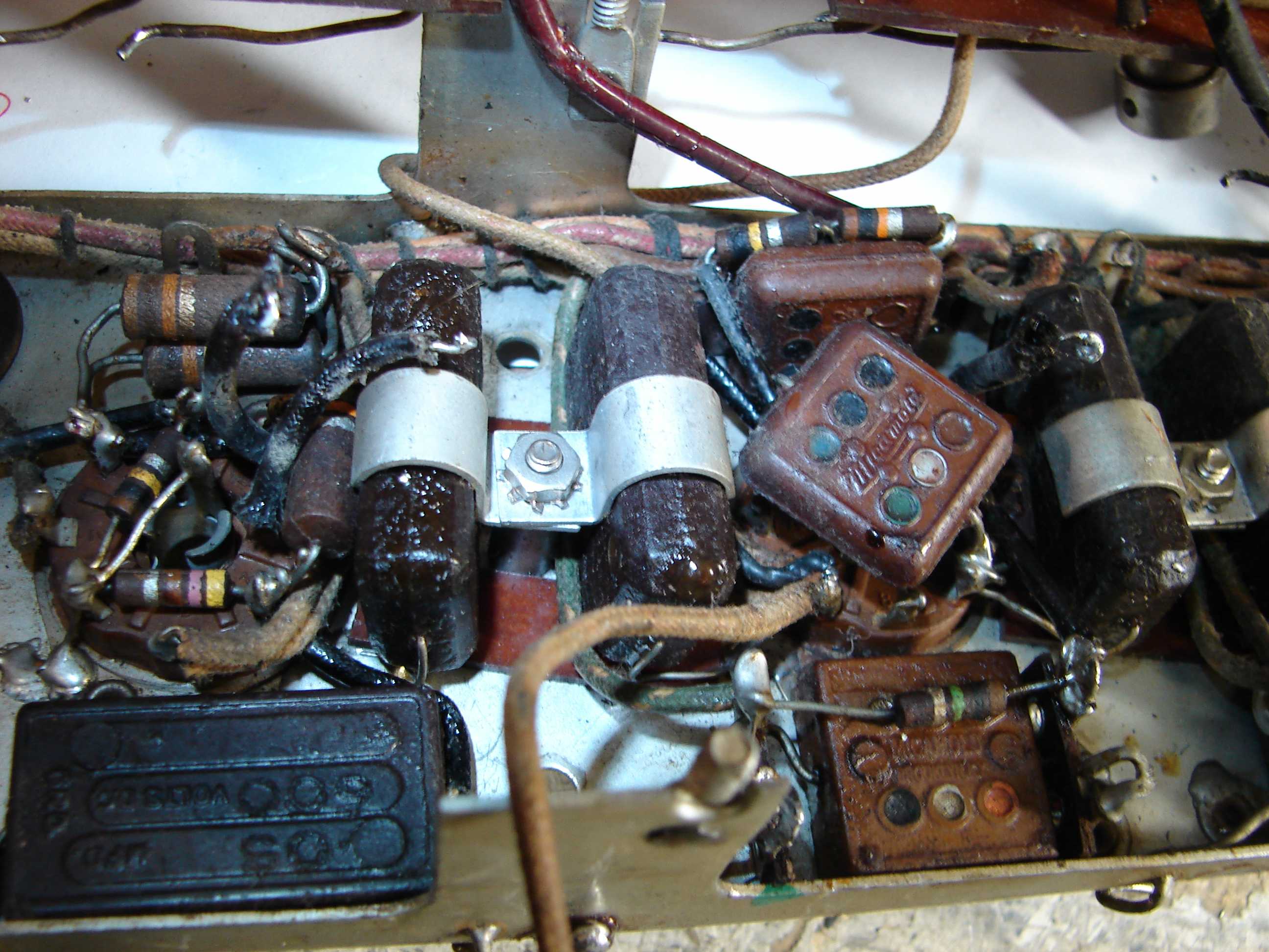
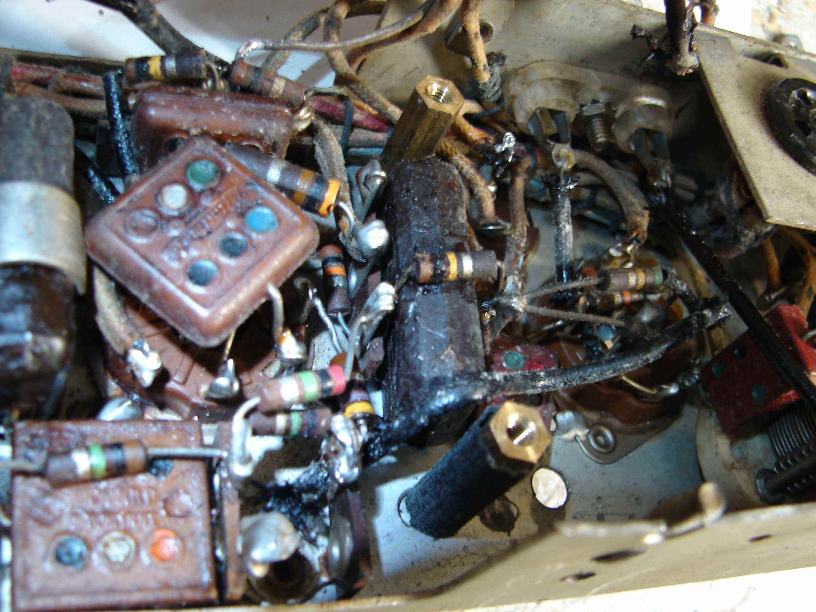
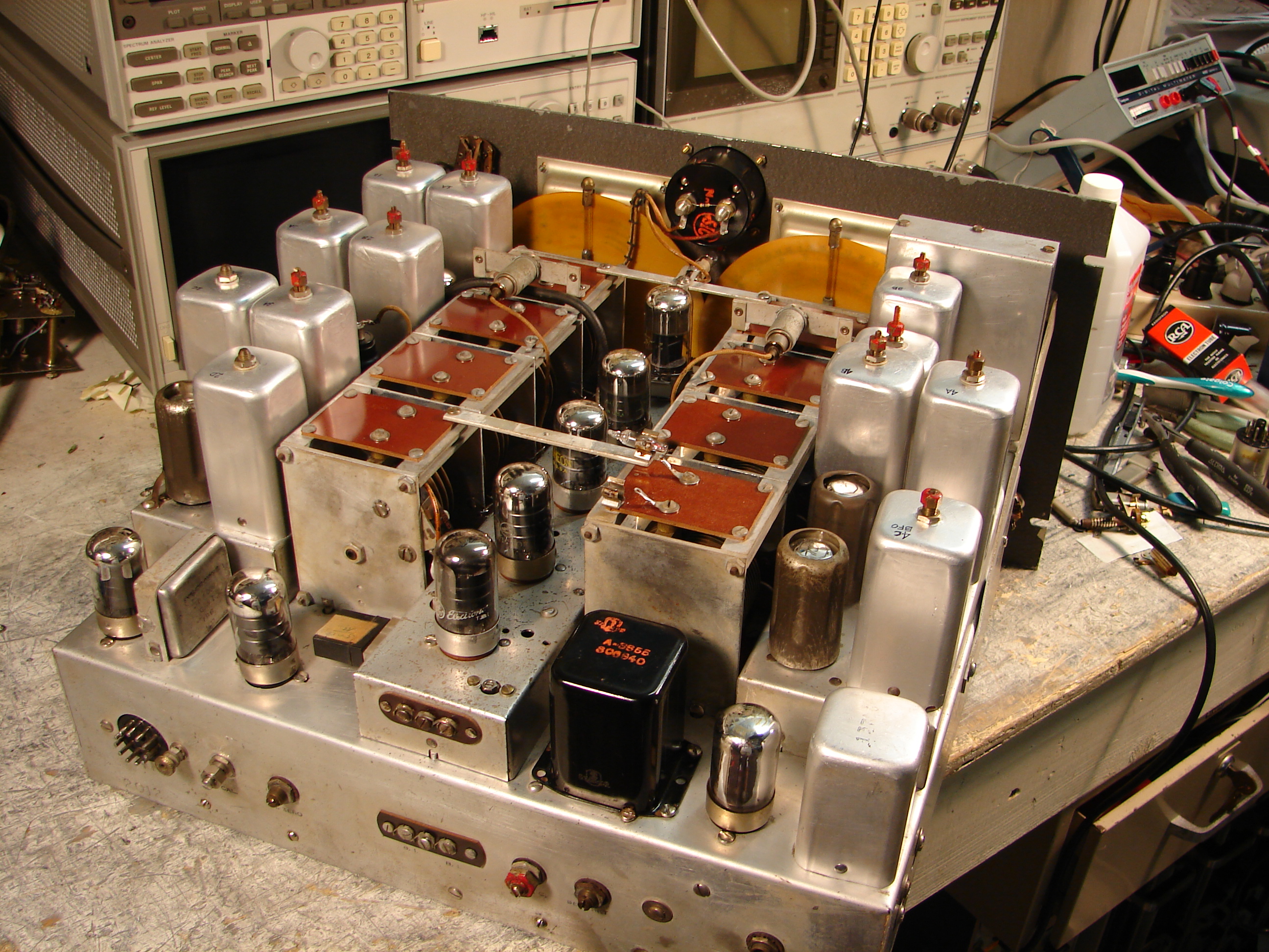
The KP-81 RF subchassis is notorious for its inaccessibility and for the high failure rate of its components. The RF subchassis consists of two chassis halves bolted together, the lower half containing the RF contact finger assembly, the upper half containing the components. The chassis halves are very closely spaced to keep component lead lengths to a minimum, making the components inside inaccessible. There is simply no way to service the KP-81 RF subchassis without first completely removing if from the receiver. Parts failures are mainly due to its 1940s vintage components—the usual oiled paper dielectric molded capacitors, molded mica capacitors, and older-style carbon composition resistors. But failures were undoubtedly increased by the fact that the RF subchassis runs much hotter than the other sections of the receiver. Out of curiosity, I checked each component during disassembly, and found that 100% of the capacitors, including the molded micas, were far out of limits for leakage current, and in many cases were so leaky that capacitance couldn’t even be measured. This was a real problem on a few capacitors whose color codes were no longer visible. All the molded paper capacitors were leaking dielectric oil. Most carbon resistors had aged 50% or more above nominal, and several were completely open. There were plenty of bad parts in the other sections of the receiver, but none were as bad as the RF subchassis. I suspect some of the capacitor failures were hastened by the Pierson factory assemblers’ practice of bending the capacitor leads sharply at the capacitor body to facilitate the high component density. This would have fractured the molded case end seals right at the time of manufacture. It wouldn’t be surprising if these receivers started failing after relatively few years.
Given the component failure rate and the difficulties in removing the RF subchassis, 100% component replacement is the only way to go. You sure don’t want to go through this ordeal a second time, so it’s worth using military grade components throughout.
The RF coil drawer must be removed to gain access to the RF subchassis mounting screws. Locate the coil drawer front track guide assembly on the center top of the chassis, directly behind the front panel. Loosen the detent ball adjustment screw and the track guide assembly mounting screws as far as practical, without removing them altogether. Carefully invert the receiver on the work bench, making sure to prevent movement of the coil drawer in the process. Support the chassis at the rear, to prevent the IF transformer adjustment screws from contacting the bench surface. Remove the metal strap covering the coil drawer carriage rod end bushing on the right rear side of the receiver, and withdraw the carriage rod from the receiver chassis through the bushing. It may help to lightly grease the carriage rod first. Note that, with the carriage rod removed, the rear of the coil drawer is unsupported, and must be handled carefully. Lift upward on the coil drawer, and move it horizontally across the receiver chassis until the coil drawer rack can be disengaged from the bandswitch gearbox pinion gear, and the drawer lifted clear of the chassis. Exercise great care not to damage the RF coil contacts or RF subchassis fingers in the process.
 |
 |
 |
| Coil drawer installed in chassis | Coil drawer removed--bottom view | Coil drawer top view showing contacts |
 |
 |
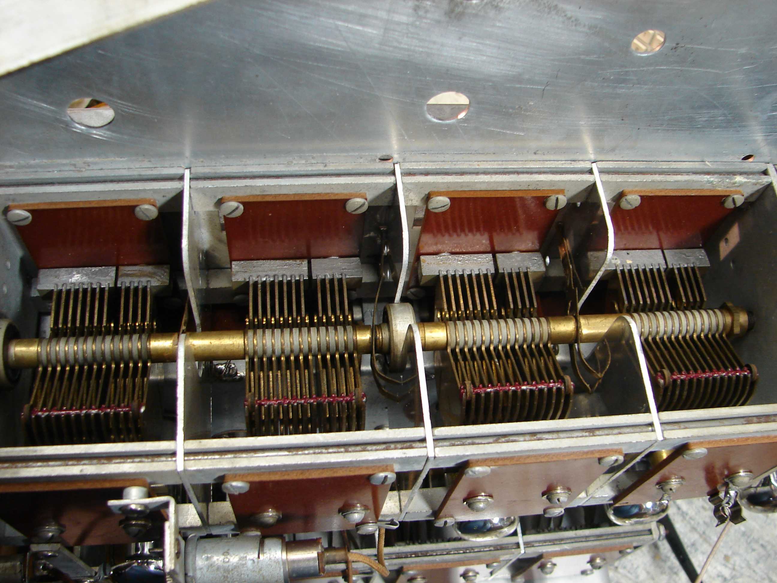 |
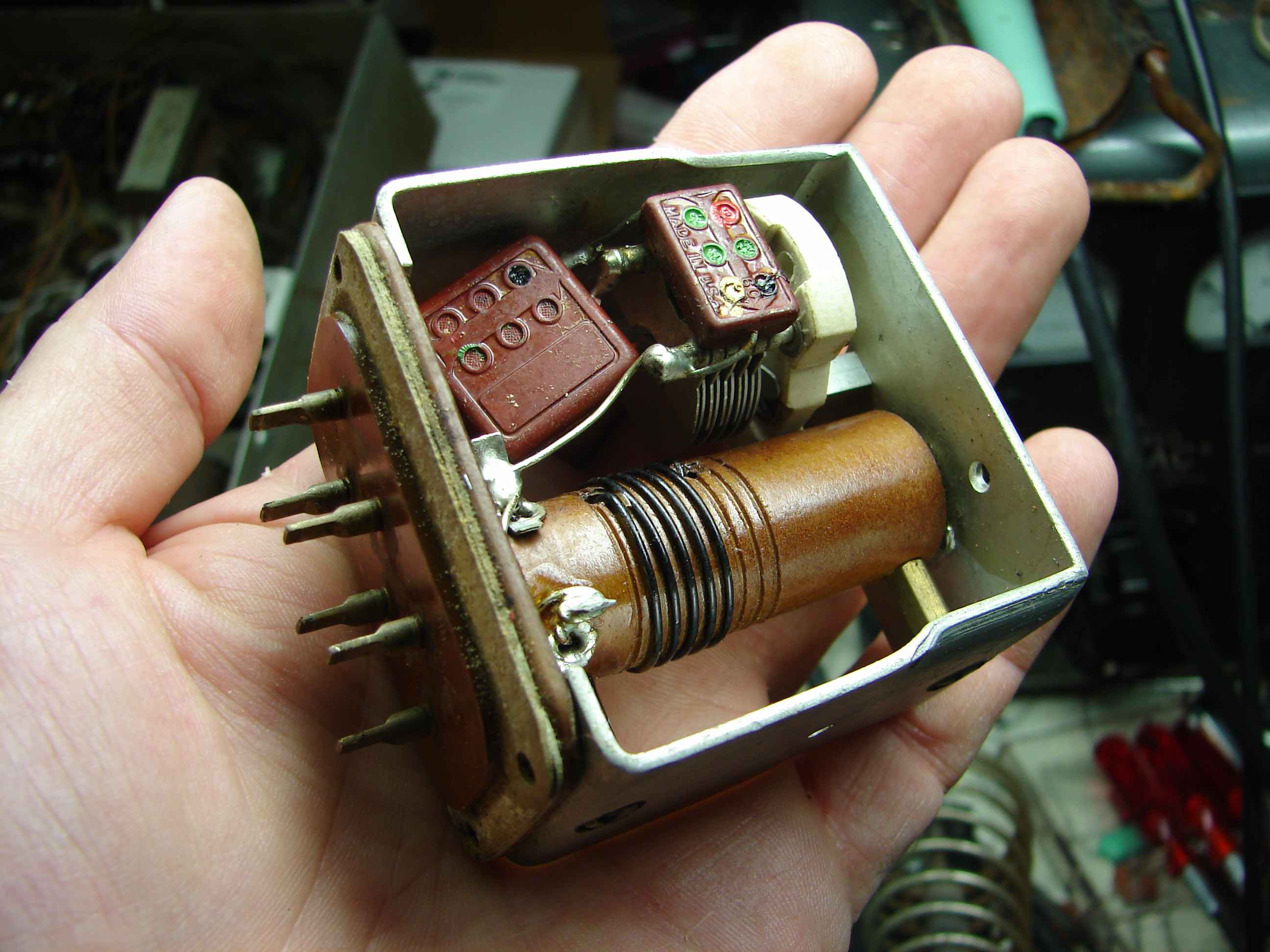
| Coil drawer lid | Local oscillator coil assembly | Tuning capacitor |
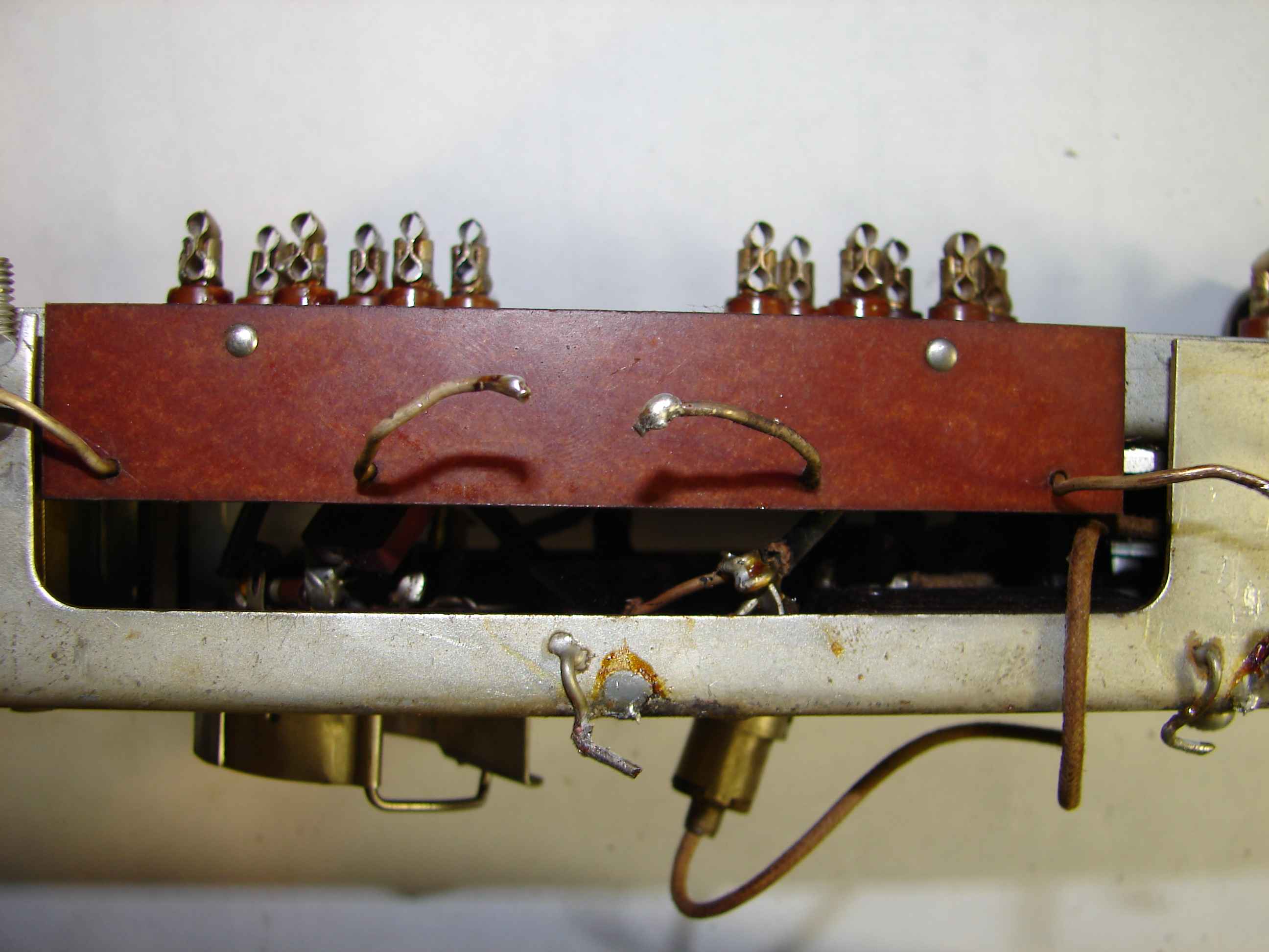
Disconnect the IF output coax cable from the RF subchassis. Unplug the 500 kc calibrator crystal, and remove the two screws attaching the calibrator microswitch S201 to the rear of the bandspread tuning capacitor, then remove and unsolder the microswitch. Unplug the lamp sockets from the dial light projectors mounted on the tuning capacitor frames. Unsolder the two front-end protection neon lamps, and remove the metal braces connecting the main and bandspread tuning capacitors at the front and rear. Unsolder the 16 wire connections between the RF subchassis and the main and bandspread tuning capacitor terminals. Unsolder the ground lugs which connect the main and bandspread tuning capacitor frames to the RF subchassis. This requires a very robust soldering iron, which you’ll also need later for soldering component ground connections inside. Remove the RF subchassis mounting screws on the bottom of the receiver chassis, and lift the RF subchassis from the top side of the receiver chassis.
The RF subchassis halves must be separated to gain access to the components inside. After removing the mounting screws on the top of the chassis, the two chassis halves can be separated just enough to permit disconnecting the components and wires which interconnect the contact finger assembly and the upper chassis half. The lower chassis half can then be swung away from the upper half, making components fully accessible.
 |
 |
 |
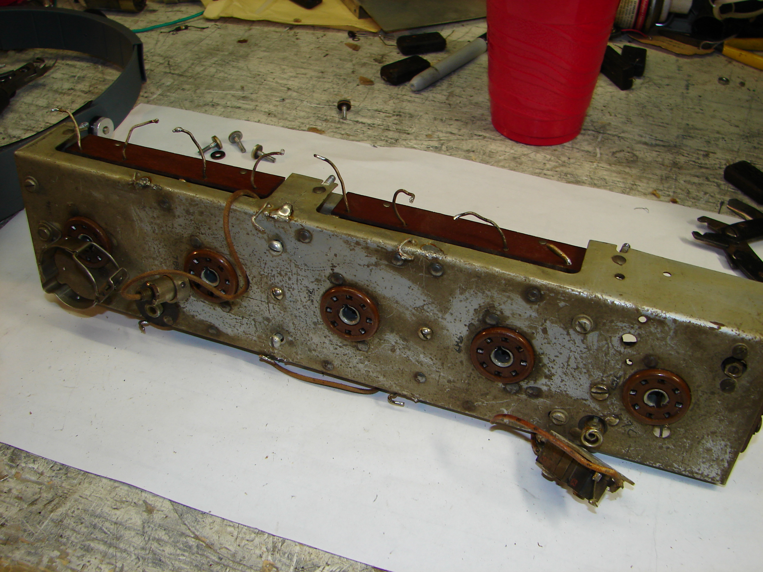
| RF Chassis top view | RF Chassis bottom view | RF Chassis separated into 2 parts |
 |
 |
 |
| RF Chassis side view | RF Chassis Components #1 | RF Chassis Components #2 |
 |
||
| Rebuilt RF Chassis Closeup |
Component choices were limited in 1946, and Pierson often used molded paper capacitors where he wanted large value RF bypasses, something no one would do today. These were inductive and had lousy Q, but there wasn’t much choice. Today, most restorers would probably replace these with a film capacitor such as the well-known Sprague "Orange Drop", but though these have much lower loss, they too are relatively inductive, which makes them poor bypasses in RF circuitry which must operate up to 40 Mc. The best choice is a CMO5 grade dipped silvered mica, though these are pretty expensive in the larger values. If you don’t want to shell out the money, a low loss ceramic such as X7R is also good, though these aren’t exactly cheap, either. It’s probably best to avoid using the much cheaper Z5U and similar ceramic types, as they’re lossier, are not temperature stable, and their capacitance varies greatly with applied voltage.
Most of the new capacitors will be much smaller than the originals, which affords some flexibility in parts placement. The usual good RF construction practices and short lead lengths should do the trick, but it’s best to keep to the original parts layout in most cases. Replacements for C205 and C212 should be soldered across the tube sockets, as they were originally. Lead dress of local oscillator and crystal calibrator components should also be duplicated. The body of C220 should be secured to the chassis with glue. Note that C201, the 500 kc calibrator output coupling capacitor, is a wire "gimmick" capacitor. It consists of an insulated wire threaded through a hole in the mounting tab of a terminal strip which lightly couples the calibrator output to the vicinity of R221 in the RF amplifier grid circuit. Avoid disturbing the original orientation.
Pierson appears to have tweaked the KP-81 design all throughout its short production lifetime, and the design probably never really stabilized before they went belly-up. Fortunately, the RF sections of the receiver seem to have undergone relatively few changes, at least through the series one and early series two receivers I’ve examined. I found relatively few component value changes, and these were noted wherever possible in the parts list I compiled for receiver number 2012. Check component values as they’re removed, since some component values may differ from the parts list. It’s probably best to stick with the component values peculiar to your receiver, especially if you have a later serial number.
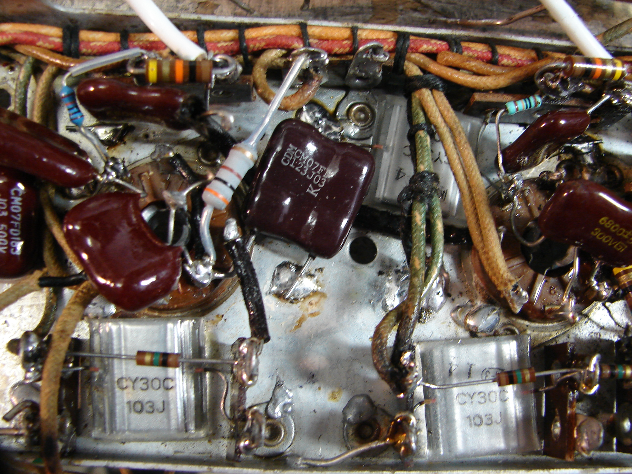
IF subchassis removal and overhaul is fairly simple. After disconnecting front panel control shafts from the IF subchassis, place the receiver on its side, and set the bandswitch to move the coil drawer to allow access to the IF subchassis mounting nuts on the receiver chassis. Unplug the connectors at the front and rear of the chassis, and remove the mounting nuts. Remove the IF subchassis from the receiver main chassis.
Like the RF subchassis, each IF subchassis is loaded with molded paper and mica capacitors, both under the chassis, and within the IF transformer cans. All of the paper types should be replaced with X7R dielectric ceramic or equivalent types. Some of the molded mica types may have survived, but these should be checked for capacitance and leakage to be sure. It’s best to replace these with modern dipped silvered mica types, especially those within the IF cans. It may be possible to retain resistors which are still within no more than 20% of their nominal values, but any which have aged beyond this should be replaced.
 |
 |
 |
| IF Chassis #1 | Xtal Filter components | IF Filter crystal |
 |
 |
|
| Another shot of IF Chassis #1 | IF Chassis #2, including Xtal Filter |
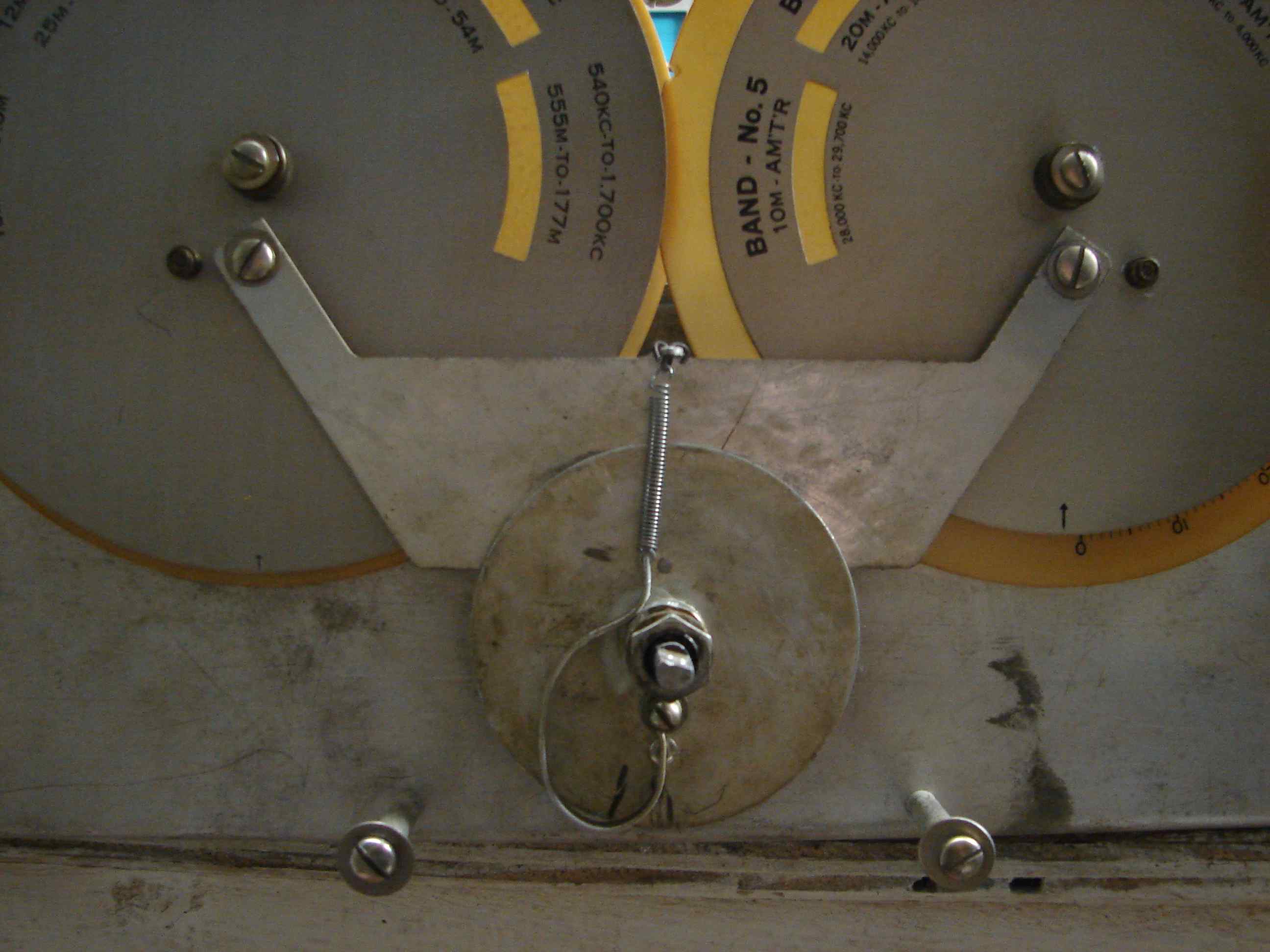
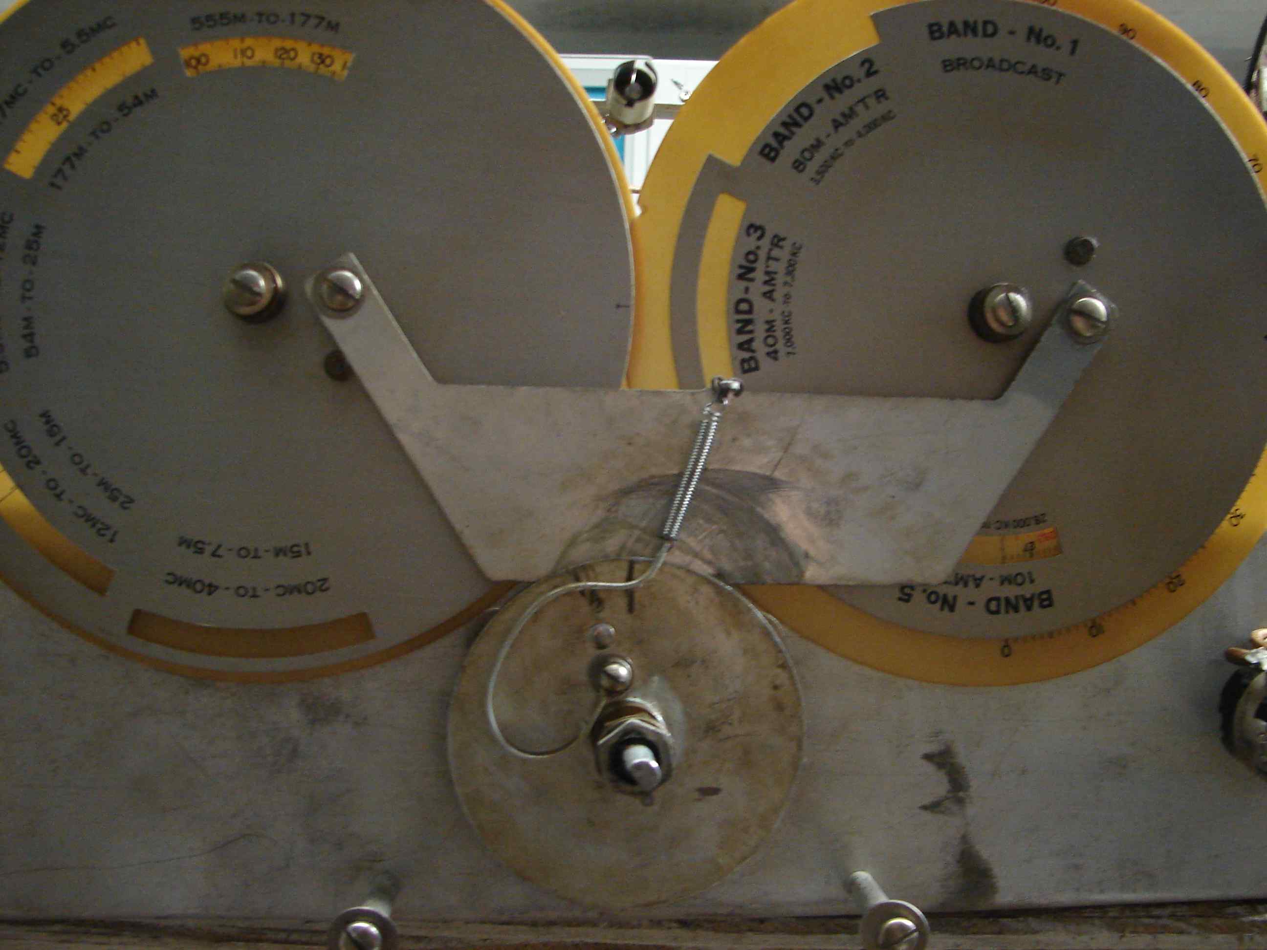
The KP-81 features an unusual drive mechanism which positions
"band in use" shutters in front of the main and bandspread tuning
dials (see accompanying pictures). The front panel bandswitch shaft passes
through two closely spaced parallel discs which have a cam plate sandwiched
between them. A roughly U-shaped shutter linkage plate connects to pivot
points on the main and bandspread dial shutters, rotating them in synchronism.
The shutter linkage plate slips down between the parallel discs and rides on the
cam, held against its surface by the tension of a spring-loaded eccentric arm
attached to the front surface of the disc assembly. When the mechanism
rotates through the cam's bottom dead center, a small "tang"
projecting from the cam surface engages a complementary notch in the bottom of
the shutter linkage plate, ensuring the proper relationship between shutters and
bandswitch position. Spring tension is important, and the eccentric arm
rotates around the bandswitch knob shaft with a complex motion which minimizes
variations in spring extension. Relatively constant spring tension is
thereby maintained over the entire rotational cycle.
Maladjustment of the shutter drive mechanism is common on the KP-81, resulting
in misalignment of the shutter openings in the display windows. Small,
consistent misalignments can usually be corrected by loosening the set screw on
the bandswitch shaft and rotating the mechanism to bring the shutters into
alignment. However, the shutters often will not return to the same
position with each subsequent rotation of the bandswitch. Here, the usual
culprit is a badly stretched tensioner spring, allowing slippage between the
shutter linkage plate and the bandswitch shaft cam. The spring must then
be replaced and the mechanism realigned. The eccentric arm may also have
become deformed (refer to the accompanying pictures as a guide to reforming a
damaged eccentric arm).
Fortunately, repair is usually a simple matter of selecting a similar spring and
cutting it down in length to obtain proper tension. For convenience, I did
this with the receiver disassembled and the coil drawer removed. However,
the job can be done with just the front panel removed. Trim the spring to
a reasonable initial length, and attach one end to the eccentric arm, the other
end to the shutter linkage plate. Engage the shutter linkage plate against
the cam surface, and rotate the mechanism until it reaches bottom dead center
and the cam tang has engaged the linkage plate notch. This
represents the Band 3 shutter position (note alignment arrows printed on shutter
discs in photo). Rotate the bandswitch through all bands, checking that
spring tension is sufficient to prevent shutter linkage plate slippage and that
shutter alignment is maintained. Note that the eccentric arm should
"wrap around" the bandswitch shaft as the mechanism rotates. If
necessary, repeat the process, cutting the spring to shorter lengths with each
iteration until the required tension is obtained.
Later, after coil drawer installation, the shutter mechanism must be
"phased" to the coil drawer position. First, pre-position the
system to Band 3. Loosen the bandswitch shaft set screw and adjust the
mechanism until the dial shutters are correctly aligned in the display window.
Tighten bandswitch set screw.
The mechanism seems unnecessarily complex, but once properly adjusted, it
functions reliably and will maintain correct shutter alignment.
 |
 |
 |
|
| Shutter drive shown in Band 5 position | Shutter drive shown in Band 3 position | Shutter drive shown in Band 1 position |
The only known KP-81 IF alignment procedures were apparently in the form of scribbled notes from Karl Pierson to a KP-81 owner many years ago, later typewritten and included with scans of the manual by Rodger, WQ9E. The following procedure is an elaboration on this note. In it, Pierson states that the swept IF response should be as follows:
I am personally skeptical of the 4.5 kc figure, and especially the 8.5 kc figure, which would have been tough to measure in those days, even if it were real. The KP-81 IF was originally sweep aligned at the factory, and for best results, alignment pass should be performed using a sweep generator and detector, or preferably a scalar or vector network analyzer (VNA). If the equipment is not available to sweep align the IF, the following procedure can be used:
- Terminate antenna terminals with a 50 ohm load. Connect an AC VTVM to the receiver 500 ohm audio output. Loosely couple an accurately calibrated signal generator to mixer tube V204. This can be done by connecting the center conductor of the generator output cable to a tube shield and placing this over V304. Ground the coax shield to an adjacent point on the chassis.
- Set crystal filter switch to "SERIES" and set crystal phasing control to "SET" position. Adjust signal generator frequency from a nominal value of 465 kc to determine center frequency of crystal filter. An accurate, frequency synthesized signal generator tuneable in 10 cps steps should be used for this, or a non-synthesized generator carefully monitored with a frequency counter.
- Set crystal filter switch to "OFF". With signal generator set to crystal filter center frequency, adjust modulation for 80% AM at 400 cps. Adjust RF output level to the minimum level required to obtain a useable meter reading. Adjust all IF transformers except 2D for maximum detected audio. Repeat as necessary until no further increase is obtained.
- Adjust 2A secondary (bottom slug) for minimum output. This peaks the grid circuit of silencer noise amplifier V304.
- Remove the grid cap of V30, thereby removing the IF signal input to V302 grid 1.
- Set front panel Silencer switch to the "FONE" position, set the receiver set to manual RF gain mode, and advance RF gain control as necessary to produce a measurable signal. Adjust the primary (bottom) of noise IF amplifier output transformer 2C for maximum recovered audio.
- Adjust IF rejection filter 2D for minimum audio.
- Repeat the adjustments of steps 6 and 7 until no further change is noted.
- Replace V302 grid cap, and check for equal recovered audio level with the Silencer switch in the OFF and FONE positions. If necessary, adjust 2A secondary slightly to equalize IF gain in both OFF and FONE positions.
This last step of equalizing receiver gain with the silencer on or off is important. If gain is sufficiently imbalanced, receiver noise can actually increase with the silencer on. The subjective effect is an increase in receiver "hiss" with the silencer on, though blanking action is still effective. The silencer also has a tendency to alter the IF passband shape. This is probably due to inadequate noise amplifier output rejection by the 2D transformer. Balancing receiver gain minimizes this effect.
I found it helped to tweak the silencer for best blanking action with impulse noise applied to the receiver front end using a pulse modulated signal generator or actual off-air impulse noise. After performing the above procedure, apply the impulse noise source to the antenna connector, and with the Silencer switch set to FONE, slightly adjust 2A secondary, and 2C for best blanking performance. This may end up being a matter of compromise between best blanking and best receiver gain balancing, depending on how "hot" your receiver’s IF is.
Peaking the IF as in the procedure above, then checking the response with a network analyzer showed this method produced suboptimal results, although it was good enough to "get by". Sweep alignment is much better, if you have the equipment available. I used a vector network analyzer with a FET probe coupled closely to detector tube V402 to recover the signal at the end of the IF strip. Before sweep alignment, perform the procedure above as an initial alignment, and then proceed as follows:
- Terminate antenna terminals with 51 ohm resistor (any value from 47 to 75 ohms is acceptable). Loosely couple the VNA swept RF source to mixer tube V204 as described above, and loosely couple the IF output to the VNA receiver using a high impedance active (FET) probe placed close to detector tube V402.
- Set Silencer switch to OFF, and RF gain to manual mode. Set VNA center frequency to 465 kc, 10 kc span. Use the minimum RF drive required to get a useable analyzer display. Adjust FET probe positioning as necessary to obtain maximum recovered IF signal, and adjust analyzer receiver reference level as needed to minimize RF drive level requirement. Use the lowest possible receiver RF gain setting needed to get a useable display indication, and avoid developing AVC action, as this will affect IF response. The R meter should not deflect upward as the signal sweeps through the IF passband.
- Set crystal filter switch to "SERIES, adjust front panel phasing control to "SET" (capacitor fully meshed). Keep sweep rate sufficiently slow to prevent scan loss.
- Observe crystal filter center frequency, and set analyzer center frequency to that value. Set crystal filter switch to OFF.
- Tune each IF transformer, primary followed by secondary (except for 2A secondary, 2C, and 2D), in sequence starting with 1A and working sequentially through 3A, to obtain maximum amplitude, best passband flatness, and overall response symmetry. Several iterations will be required to obtain the desired response. Do not adjust 2A secondary, 2C, and 2D during this process.
- Once a desirable IF response has been achieved, tune 2A secondary for minimum amplitude. If this alters the IF response, repeat step 5 as necessary to restore correct response.
- Turn off IF sweep drive, but leave RF sweep injection connections to mixer V204. Remove antenna termination resistor and connect RF impulse noise source to antenna terminals. Tune receiver to RF noise source, and set Silencer switch to FONE.
- Adjust primary and secondary of transformer 2C, and IF rejection filter 2D for best impulse noise blanking. Slightly retouch 2A secondary setting as needed for best impulse noise blanking.
- Disconnect RF noise source, set Silencer switch to OFF. Reconnect antenna termination resistor.
- Turn on IF sweep drive again, and retouch IF transformers, if necessary (except 2A secondary, 2C, and 2D), for maximum amplitude and best IF response shape.
- Set Silencer switch to FONE. Amplitude of IF response should not change by more than 3 dB in FONE or OFF positions of Silencer switch.
- Set BFO tuning capacitor VC402 to half-mesh, and with the front panel BFO knob set screws loosened, orient the BFO knob on the tuning capacitor shaft so that the knob skirt index is at "0" on the front panel BFO dial plate.
- Couple an accurate 465 kc unmodulated test signal to mixer tube V204, adjusting signal generator amplitude and coupling to obtain a mid scale R-meter reading.
- Adjust BFO coil L408 for zero beat in the received audio.
- Tighten L408 leadscrew locknut, and tighten BFO knob set screws.
The passage of over 65 years and the replacement of mica capacitors in the RF coil modules guarantees that front end and L.O. alignment and tracking adjustments will be needed. Unfortunately, after completing RF alignment at the factory, the Pierson factory techs tightened down the L.O. tuning inductor leadscrew locknuts, then cut the leadscrews off right at the top of the locknuts. They did this to avoid clearance problems between the ends of the lead screws and the bottom chassis cover, but in doing so made it impossible to get a tuning tool on the inductors. It seems they didn’t think the receiver would ever need realignment. In my receiver, tracking adjustments required that the L.O. inductor slugs be turned further into the coils, making matters worse. The solution was to back out the slugs and cut a new slot in the ends of the leadscrews so they could be readjusted as needed. After removing each locknut, I cleaned up and flattened the end of the leadscrew with a file, then cut a new slot in it with a very thin diamond cutting disk on a Dremel Moto-Tool. Needless to say, this must be done carefully, with the leadscrew minimally extended beyond the locknut to avoid damaging the leadscrew.
After prepping the L.O. inductor leadscrews, connect an RF signal generator to the antenna terminals, and tune it and the receiver to the upper frequency of band being aligned.
- Tune the OSC trimmer capacitor at the upper band edge until the local oscillator is on-frequency, and the signal generator is received at maximum level.
- Adjust the ANT, RF, and MOD (mixer) trimmer capacitors for maximum signal. Repeat until no further improvement is attained. Back off signal generator level to minimum needed to make the adjustment.
- Tune generator and receiver to bottom edge of the band, and adjust the OSC inductor leadscrew for max received signal.
- Retune the receiver to the upper band edge frequency, and all trimmer capacitors for maximum.
- Repeat steps 1-4 until no further improvement is obtained.
- Secure OSC leadscrew locknuts, making sure not to disturb leadscrew setting.
- Proceed to next band, and repeat the entire procedure.
Since the ANT, RF and MOD coils are not adjustable, it may be difficult to obtain good tracking between the L.O. and the other RF circuits. It may be worth experimenting with changing the upper and lower alignment frequencies, to obtain the best compromise in L.O./RF tracking. The only other recourse is slight "knifing" of the segmented tuning capacitor plates. This is of limited utility, as some bands may track differently than others, and it may be best to leave well enough alone.
 |
 |
 |
| Restored KP-81 front view | Restored KP-81 rear view | Closeup of panel |
Notes:
- Resistors are 1/2W 10% carbon composition unless noted otherwise
- "SM"=silvered mica
REF. DES. |
DESCRIPTION |
REMARKS |
| R201 | 51K | |
| R202 | 510K | |
| R203 | 220K | |
| R204 | 1M | |
| R205 | 100K | |
| R206 | 300 ohm 1W | |
| R207 | 1M | |
| R208 | 300 ohm 1W | |
| R209 | 470 ohm | |
| R210 | 100K | |
| R211 | 15K 1W | |
| R212 | 47 ohm | |
| R213 | 24K | |
| R214 | 24K | V205 screen resistor |
| R215 | 100K | R215 assigned twice, screen resistor, V202 |
| R215 | 1M | R215 assigned twice, AGC time constant resistor |
| R216 | 10K | |
| R217 | 100K | |
| R218 | 10K | |
| R219 | 10K | |
| R220 | 2M | R220 assigned twice, AGC bias resistor |
| R220 | 10K, 1W | R220 assigned twice, V204 grid 5 resistor. Some receivers may have 51K installed |
| R221 | 10K, 1W | R221 assigned twice Some receivers may have 51K installed |
| R221 | 47 ohm | R221 assigned twice, 1st RF amp grid parasitic suppression resistor |
| R222 | 1K, 1W | V205 plate resistor. Reference designator missing, |
| R222 | not assigned | |
| VC201 | air variable | |
| C201 | wire "gimmick" | capacitor free wire end loosely couples xtal calibrator output to junction of R204 and R221 (47 ohm) |
| C202 | 500 pF 500V SM | |
| C203 | 10 pF 500V SM | |
| C204 | 200 pF 200V SM | some receivers may have 20 pF installed |
| C205 | 0.05 uF 200V paper | V202 screen grid bypass |
| C206 | 100 pF 500V SM | V202 grid coupling |
| C207 | 0.1 uF 300V paper | V202 cathode bypass |
| C208 | 6000 pF 500V SM | V202 plate decoupling |
| C209 | 100 pF 500V | SM Not assigned |
| C210 | 0.01 uF 300V paper | V203 cathode bypass |
| C211 | 0.01 uF 200V paper | V203 screen bypass |
| C212 | 6000 pF 500V SM | V203 screen to cathode |
| C213 | 6000 pF 500V SM | V203 plate decoupling |
| C214 | 0.01 uF 500V paper | V204 grid 5 bypass |
| C215 | 250 pF500V 5% | L.O. grid coupling |
| C216 | 6000 pF 500V SM | L.O. screen bypass |
| C217 | 0.01 uF 500V paper | L.O. plate decoupling |
| C218 | Not assigned | |
| C219 | 0.01 uF 500V paper | |
| C220 | 100 pF 500V 5% | C220 assigned twice. L.O. plate blocking to V204 mixer grid |
| C231 | 0.5 uF 500V paper | C231 assigned twice, mixer cathode bypass |
| C231 | 0.01 uF 500V paper | C231 asssigned twice, AGC time constant |
REF. DES. |
DESCRIPTION |
REMARKS |
| C220 | 600 pF 500V 2% SM | C220 assigned twice. In Band 1 osc compartment |
| C221 | 1500 pF 500V 2% SM | Band 2 oscillator compartment |
| C222 | 2500 pF 500V 2% SM | Band 3 oscillator compartment |
| C223 | 2100 pF 500V 2% SM | Band 4 oscillator compartment |
| C224 | 25 pF 500V 2% SM | Band 4 antenna padder |
| C225 | 30 pF ceramic, axial lead | Band 4 RF compartment |
| C226 | 25 pF 500V 2% SM | C226 assigned twice. Band 4 mixer secondary padder (mod compartment) |
| C226 | 4000 pF parallel with 5000 pF | C226 assigned twice. Band 5 osc. Compartment Both 500V 5% SM |
| C227 | Not assigned | |
| C228 | 25 pF 500V 2% SM | Band 4 oscillator padder |
| C229 | 250 pF 500V 5% SM | Band 5 RF coil top coupling |
| C230 | 240 pF 500V 2% SM | Mixer primary/secondary top coupling |
| C231 | 0.5 uF 500V paper | C231 assigned twice, mixer cathode bypass |
| C231 | 0.01 uF 500V paper | C231 asssigned twice, AGC time constant |
REF. DES. |
DESCRIPTION |
REMARKS |
| C302 | 0.05 uF 500V paper | |
| C303 | 100pF, 500V 5%, SM & 10 pF 200V 10%, SM | Two capacitors in parallel |
| C304 | 0.05 uF 600V paper | |
| C305 | 2500 pF 500V, SM | |
| C306 | 240 pF 500V 5% SM & 200 pF 200V 5% SM | Two capacitors in parallel |
| C307 | 100 pF 500V 5% SM | |
| C308 | 200 pF 200V 5% SM | |
| C309 | 200 pF 500V 2% SM | |
| C310 | 0.05 uF 200V paper | |
| C311 | 0.01 uF 500V paper | |
| C312 | Not assigned | |
| C313 | 200 pF 500V 2% SM | |
| C314 | 0.02 uF 600V paper | |
| C315 | 0.05 uF 600V paper | V302 cathode bypass |
| C316 | 200 pF 500V, 2% SM | 2B IF primary capacitor |
| C317 | 200 pF 500V 2% SM | |
| C318 | 200 pF 500V 2% SM | 2A IF Primary |
| C319 | 0.05 uF 500V paper | Screen grid bypass for V301 and V305. Actually located at V305 pin 3. |
| C320 | 0.01 uF 500V paper | |
| C321 | 0.02 uF 600V paper | |
| C322 | 0.02 uF 600V paper | |
| C323 | 200 pF 500V 2% SM | |
| C324 | 0.02 uF 600V paper | |
| C325 | 0.02 uF 600V paper | C325 assigned twice. |
| C325 | 0.01 uF 600V paper | C325 assigned twice. 2nd screen grid bypass for V301 |
| C326 | 200 pF 500V 2% SM | |
| C327 | 200 pF 500V 2% SM | |
| C328 | 200 pF 500V 2% SM | |
| C329 | 0.05 uF 600V paper | |
| C330 | 250 pF 500V 5% SM | C330 assigned twice. V304 screen bypass. |
| C330 | 0.02 uF 600V paper | C330 assigned twice. V302 grid #3 coupling capacitor |
| C331 | 2000 pf 200V SM | |
| R301 | 240K | |
| R302 | 750 ohm | Some receivers may have 820 ohm here |
| R303 | Not assigned | |
| R304 | 100K 1W 10% | |
| R305 | 240K | Connects bottom 2C IF scondary |
| R306 | 10K | Connects to bottom of 2C IF primary |
| R307 | 10K | |
| R308 | 1M | |
| R309 | 51K, 1W | |
| R310 | 2.4K | |
| R311 | 100K | |
| R312 | 1M | |
| R313 | 10K | |
| R314 | 10K | |
| R315 | 470 ohm | |
| R316 | 1K | |
| R317 | 100K V302 | Grid 3 to ground |
| R318 | Not assigned | |
| R319 | 100K | connects bottom of 1B IF secondary |
| R320 | Not found | Additional cathode resistor for V301. Shown on schematic, but not found in either of two receivers inspected |
REF. DES. |
DESCRIPTION |
REMARKS |
| C401 | 200 pF 200V 5% SM | |
| C402 | 0.01 uF 600V paper | C402 not originally assigned. C402 arbitrarily assigned here to unmarked cap at bottom of 3B IF transformer primary |
| C403 | 400 pF 500V 2% SM | |
| C404 | 400 pF 500V 2% SM | |
| C405 | "gimmick" capacitor | capacitance between lugs on ceramic spacers of IF XTAL |
| C406 | 51 pF tubular ceramic | selected part, probably for best match with IF crystal |
| C407 | 0.01 uF 600 V paper | |
| C408 | 200 pF 500V 2% SM | |
| C409 | 500 pF 500V 5% SM | |
| C410 | 0.05 uF 600V paper | |
| C411 | 200 pF 500V 2% SM | |
| C412 | 200 pF 500V 2% SM | |
| C413 | 200 pF 500V 2% SM | |
| C414 | 0.01 uF 600V paper | |
| C415 | 200 pF 500V 2% SM | |
| C416 | 500 pF 500V 5% SM | |
| C417 | 0.02 uF 600V paper | |
| C418 | 0.05 uF 500V paper | |
| C419 | 250 pF 500V 5% SM | in parallel with R408 in BFO section |
| C420 | 200 pF 500V 2% SM | |
| C421 | 0.05 uF 600 V paper | |
| C422 | 10,000 pF tubular ceramic | C422 assigned twice. In detector filter. |
| C422 | 0.05 uF 600V paper | C422 assigned twice. Bypass cap. In 4A IF can primary |
| C424 | 0.1 uF 250V paper | Arbitrarily assigned reference designator for unmarked v401 cathode bypass capacitor |
| C423 | 100 pF 500V 5% SM | |
| VC401 | 2-24 pF air variable | |
| VC402 | 2-24 pF air variable | BFO Pitch |
| R401 | 10k | |
| R402 | 300 Ohm | |
| R403 | 10K | |
| R404 | 10K | |
| R405 | 100K | |
| R406 | 100K | |
| R407 | 10K | |
| R408 | 10K | |
| R409 | 51K 1W | |
| R410 | 100K | |
| R411 | 360K | |
| L409 | 270 mH | DC resistance 450 ohms |
| REF. DES. | DESCRIPTION | REMARKS |
| R101 | 510K | |
| R102 | 250M | |
| R103 | 1K | Audio Volume pot |
| R104 | 510K | |
| R105 | 510K | V102 grid resistor |
| R106 | 1K pot, wirewound | R Meter Calibration pot |
| R107 | 100 ohm 1W | |
| R108 | 25 megohms | Squelch Control pot |
| R109 | Not assigned | |
| R110 | 25 megohms | Manual Volume pot |
| R111 | 1k 2W | Sensitivity Set pot |
| R112 | 300 ohm 1W | V101 cathode resistor |
| R113 | 51 ohm 1W | R meter shunt |
| R114 | top to bottom=8.07K | multiple-tapped wirewound power resistor, 1st tap to bottom=3.65K, 2 nd tap to bottom=350 ohm |
| R115 | 200 ohm R | Meter Zero pot |
| R116 | 1 M | |
| R117 | 240K | |
| R118 | 1M | AVC Zero Set pot |
| R119 | 240K | |
| R120 | 130K, 1W | audio LPF |
| R121 | 47K | audio LPF |
| R122 1 | 5K | audio LPF |
| R123 | 130K, 1W | audio HPF |
| R124 | 68K | audio HPF |
| R125 | 24K | audio HPF |
| R126 | Not assigned | |
| R127 | Not assigned | |
| R128 | 1K | |
| R130 | 470 ohm | R130 assigned twice. From R111 wiper to gnd |
| R130 | 100K | R130 assigned twice. AVC time constant resistor (between C111 and C103) |
| C101 | 0.1 uF 600 V paper | Audio Volume pot coupling |
| C102 | Not Assigned | |
| C103 | 0.5V 600V paper | bathtub type |
| C104 | 0.5V 600V paper | bathtub type |
| C105 | 1 uF 600V | |
| C106 | 0.5V 600V paper | bathtub type |
| C107 | Not Assigned | |
| C108 | 10,000 pF | audio HPF (tubular ceramic type) |
| C109 | 2500 pF | audio HPF |
| C110 | 10,000 pF tubular ceramic | audio HPF |
| C111 | 0.5V 600V paper | bathtub type |
| C112 | 500 pF 500V 5% |
| REF. DES. | DESCRIPTION | REMARKS |
| R501 | 100K | |
| R505 | 10K | |
| R506 | 560 ohm | |
| R507 | 10K | |
| R508 | 4.7K 2W | |
| R509 | 4.3K | guesstimated 5W |
| R510 | 780 ohm | guesstimated 5W |
| C501 | 10uF 450V electrolytic | |
| C502 | 10uF 450V electrolytic | |
| C507A,B | 20 uF 450V electrolytic | |
| C508A,B | 20 uF 450V electrolytic | |
| C509 | 20uF 450V electrolytic | |
| C510 | 6000 pF 500V SM | |
| C511 | 6000 pF 600V paper | |
| C512 | 6000 pF 600V paper | |
| SPKR | 501 Jensen PM10C, 10", 8 ohm permanent magnet loudspeaker. | Some receivers may have field-coil loudspeaker. |